Abstract
Copper selenide thin films have emerged as a versatile class of materials with significant potential in energy conversion technologies, particularly in photovoltaics and thermoelectrics. This article provides a comprehensive review of recent advances in copper selenide thin films, covering their structural properties, fabrication methods, and applications in both photovoltaic and thermoelectric devices. The review highlights the remarkable progress in achieving high-efficiency solar cells based on copper selenide compounds and the development of high-performance thermoelectric thin films for flexible energy harvesting applications. Recent breakthroughs in material engineering, phase control, and device integration are discussed, along with future research directions for advancing these promising materials toward commercial applications.
Table of Contents
- What is copper(I) selenide (Cu₂Se)?
- Structural Properties and Phase Transitions
- Fabrication Methods and Processing Techniques
- Photovoltaic Applications
- Thermoelectric Applications
- Recent Breakthroughs and Innovations
- Challenges and Future Perspectives
- Conclusion
- References
1. What is copper(I) selenide (Cu₂Se)?
1.1 Research Background
Copper selenide (Cu₂Se) and related compounds have attracted considerable attention in recent years due to their unique combination of properties that make them suitable for various energy conversion applications [1]. These materials exhibit excellent optoelectronic properties, tunable electrical conductivity, and relatively low thermal conductivity, making them promising candidates for both photovoltaic and thermoelectric applications. The earth-abundant nature of copper and selenium, combined with their non-toxic characteristics, further enhances their appeal for sustainable energy technologies [2].
1.2 Material Versatility
The versatility of copper selenide thin films stems from their ability to exist in multiple phases and stoichiometries, including CuSe, Cu₂Se, Cu₂₋ₓSe, and Cu₃Se₂, each with distinct electronic and optical properties [3]. This structural flexibility allows for precise tuning of material properties through composition control and processing conditions, enabling optimization for specific applications.
1.3 Research Scope
This review systematically examines recent advances in copper selenide thin film research, focusing on:
- Structural properties and phase transitions critical for device performance
- Fabrication methods including physical vapor deposition and solution-based approaches
- Applications in photovoltaic and thermoelectric energy conversion
- Recent innovations in material engineering and device integration
- Future challenges and research directions for commercial deployment
2. Structural Properties and Phase Transitions
2.1 Phase Behavior
Copper selenide thin films exhibit complex structural behavior with multiple phase transitions that significantly influence their electronic and thermal properties. The α-phase of Cu₂Se, which is stable at room temperature, transforms to a superionic β-phase at approximately 400 K, characterized by high ionic conductivity of copper ions [4]. This phase transition is accompanied by significant changes in electrical and thermal transport properties, making it particularly interesting for thermoelectric applications.
2.2 Structural Control
Recent studies have demonstrated that the structural orientation of copper selenide thin films can be controlled through deposition parameters and post-processing treatments. For instance, (001)-oriented Cu₂₋ᵧSe thin films grown by pulsed laser deposition have shown tunable thermoelectric performances, with orientation-dependent transport properties [5]. The ability to control crystal orientation and phase composition through processing conditions provides a powerful tool for optimizing material properties for specific applications.
2.3 Phase Stability
The phase stability and transformation behavior of copper selenide thin films are strongly influenced by deposition methods and post-deposition treatments. Chemical bath deposition, thermal evaporation, and sputtering techniques have been employed to produce films with controlled phase compositions and microstructures [6]. Understanding and controlling these phase transitions is crucial for achieving reproducible and high-performance devices.
3. Fabrication Methods and Processing Techniques
3.1 Physical Vapor Deposition Methods
3.1.1 Thermal Evaporation
Thermal evaporation has been widely used for depositing copper selenide thin films due to its simplicity and ability to produce uniform coatings. Recent studies have investigated the effect of film thickness on the thermoelectric properties of thermally evaporated Cu₂₋ₓSe thin films, revealing thickness-dependent optimization of power factors [7]. The evaporation process allows for precise control of composition and morphology, making it suitable for both photovoltaic and thermoelectric applications.
3.1.2 Magnetron Sputtering
Sputtering techniques, particularly magnetron sputtering, have emerged as promising methods for producing high-quality copper selenide thin films with controlled stoichiometry and microstructure. The α-Cu₂Se thermoelectric thin films prepared by copper sputtering into selenium precursor layers have demonstrated excellent thermoelectric performance with power factors reaching 9.23 μWcm⁻¹K⁻² [8]. This approach enables room-temperature fabrication followed by controlled annealing to achieve desired phase and crystallinity.
3.2 Solution-Processed Methods
Solution-based deposition methods have gained significant attention for their potential in low-cost, large-area fabrication of copper selenide thin films. Solution-processed Cu₂Se nanocrystal films have demonstrated bulk-like thermoelectric performance, with ZT values approaching those of bulk materials [9]. These methods offer advantages in terms of material utilization, processing flexibility, and compatibility with various substrates, including flexible polymers.
Layer-by-layer combination reaction methods have been developed for fabricating high-performance copper selenide thermoelectric thin films on flexible substrates [2]. This approach enables precise control of film composition and microstructure, resulting in films with high power factors (5.3 mWcm⁻¹K⁻²) and good flexibility for wearable applications.
3.3 Chemical Deposition Techniques
Chemical bath deposition (CBD) remains a popular method for producing copper selenide thin films due to its simplicity and cost-effectiveness. Recent advances in CBD have focused on controlling phase composition through pH adjustment and precursor concentration optimization [10]. Electrochemical deposition methods have also been developed for producing copper selenide films with controlled morphology and composition for various applications.

4. Photovoltaic Applications
4.1 Copper Indium Gallium Selenide (CIGS) Solar Cells
Copper indium gallium selenide (CIGS) thin-film solar cells represent one of the most successful applications of copper selenide compounds in photovoltaics. These devices have achieved remarkable efficiencies, with certified world record efficiencies exceeding 20% [11]. The CIGS technology combines the excellent optoelectronic properties of copper selenide with the bandgap tunability provided by indium and gallium alloying, resulting in high absorption coefficients and suitable bandgaps for solar energy conversion.
Recent advances in CIGS fabrication have focused on improving material quality, interface engineering, and device architecture. The development of standardized process sequences and optimized deposition parameters has enabled reproducible production of high-efficiency devices [11]. Interface quality improvement through copper-depletion layer formation has been shown to enhance device performance by reducing recombination losses.
4.2 Emerging Copper Selenide-Based Photovoltaics
Beyond CIGS, other copper selenide compounds have shown promise for photovoltaic applications. Cu₂SnSe₃ (CTSe) thin films have attracted attention as potential absorber materials for thin-film solar cells due to their suitable bandgap (approximately 1.0 eV) and high absorption coefficient [12]. Recent research has focused on understanding the growth mechanisms, phase formation, and defect properties of CTSe films to improve their photovoltaic performance.
Copper zinc tin selenide (CZTSe) represents another promising material system that combines earth-abundant elements with suitable optoelectronic properties for photovoltaic applications. The investigation of selenium-ion concentration on the optoelectronic properties of Cu₂ZnSn(S₁₋ₓSeₓ)₄ thin films has provided insights into composition optimization for improved device performance [13].
4.3 Interface Engineering and Device Optimization
Recent advances in copper selenide-based photovoltaics have emphasized the importance of interface engineering and device architecture optimization. The formation of high-quality heterojunctions with appropriate buffer layers, such as CdS or ZnSe, has been crucial for achieving high-efficiency devices [14]. Additionally, the development of transparent conducting oxide contacts and anti-reflection coatings has contributed to improved light management and reduced optical losses.
5. Thermoelectric Applications
5.1 High-Performance Thermoelectric Thin Films
Copper selenide has emerged as a promising thermoelectric material due to its combination of high electrical conductivity, moderate Seebeck coefficient, and relatively low thermal conductivity. Recent advances have focused on developing high-performance copper selenide thermoelectric thin films for flexible applications [2]. Solution-processable high-performance thermoelectric copper selenide thin films have demonstrated excellent thermoelectric properties with ZT values suitable for practical applications [3].
The development of flexible thermoelectric devices based on copper selenide thin films has opened new opportunities for wearable energy harvesting and thermal management applications. These devices can convert body heat or environmental temperature gradients into electrical energy, providing power for low-power electronics and sensors [15].
5.2 Composition and Structure Optimization
The thermoelectric properties of copper selenide thin films can be optimized through composition control and structural engineering. The effect of copper content on the electrical properties of evaporated Cu-Se thermoelectric films has been systematically investigated, revealing optimal compositions for maximum thermoelectric performance [16]. Copper-deficient compositions (Cu₂₋ₓSe) have shown particularly promising thermoelectric properties due to their enhanced carrier concentration and reduced thermal conductivity.
Nanostructuring approaches have been employed to further improve the thermoelectric performance of copper selenide thin films. The incorporation of nanoinclusions, such as PbSe nanoparticles in Cu₂₋ₓSe thin films, has been shown to enhance thermoelectric properties through phonon scattering and carrier filtering effects [17]. These multiphase systems offer opportunities for synergistic optimization of electrical and thermal transport properties.
5.3 Flexible Thermoelectric Devices
The development of flexible thermoelectric devices based on copper selenide thin films represents a significant advancement in wearable energy harvesting technology. Flexible pCu₂Se-nAg₂Se thermoelectric devices fabricated via in situ conversion from printed copper patterns have demonstrated stable performance under bending conditions [18]. These devices combine the excellent thermoelectric properties of copper selenide with the flexibility required for integration into wearable systems.
Layer-by-layer fabrication methods have enabled the production of copper selenide-based thin films with good mechanical flexibility and stable thermoelectric performance [2]. These films maintain their electrical and thermal properties under repeated bending cycles, making them suitable for integration into flexible electronics and textile-based applications.

6. Recent Breakthroughs and Innovations
6.1 Phase-Controlled Fabrication
Recent innovations in phase-controlled fabrication have enabled precise control of copper selenide thin film properties. The development of methods for producing α-phase Cu₂Se thin films with controlled orientation has led to significant improvements in thermoelectric performance [8]. These approaches involve careful control of deposition parameters and post-deposition annealing conditions to achieve desired phase purity and crystal orientation.
6.2 Hybrid and Composite Materials
The development of hybrid and composite materials combining copper selenide with other functional materials has opened new avenues for performance enhancement. High-performance thermoelectric silver selenide thin films cation-exchanged from copper selenide templates have demonstrated exceptional thermoelectric properties [19]. This approach leverages the structural template provided by copper selenide while incorporating silver to enhance electrical transport properties.
6.3 Scalable Manufacturing Approaches
Recent advances in scalable manufacturing approaches have addressed the challenge of producing copper selenide thin films for commercial applications. Solution-based processing methods, including inkjet printing and roll-to-roll coating, have been developed for large-area fabrication of copper selenide thin films [20]. These approaches offer advantages in terms of material utilization, processing speed, and compatibility with flexible substrates.
7. Challenges and Future Perspectives
7.1 Stability and Reliability
Despite significant progress, challenges remain in the long-term stability and reliability of copper selenide thin films, particularly for thermoelectric applications. The phase transitions and copper ion mobility in these materials can lead to performance degradation over time under operating conditions. Future research should focus on developing stabilization strategies, such as encapsulation layers and compositional modifications, to enhance device longevity.
7.2 Efficiency Improvements
For photovoltaic applications, further efficiency improvements are needed to compete with established technologies. Research directions include bandgap engineering through alloying, defect passivation strategies, and advanced device architectures such as tandem cells. Interface engineering and contact optimization will also play crucial roles in pushing efficiency limits.
7.3 Integration and System-Level Applications
The integration of copper selenide thin films into complete energy systems represents an important future direction. For thermoelectric applications, this includes the development of complete thermoelectric modules with optimized thermal management and electrical interconnection. For photovoltaic applications, integration with energy storage systems and smart grid technologies will be important for practical implementation.
7.4 Sustainability and Environmental Impact
Future research should address the sustainability aspects of copper selenide thin film technology, including material sourcing, manufacturing processes, and end-of-life considerations. The development of recycling methods and the use of environmentally benign processing techniques will be important for ensuring the long-term sustainability of these technologies.
8. Conclusion
Copper selenide thin films have demonstrated remarkable potential for both photovoltaic and thermoelectric applications, driven by their excellent optoelectronic properties, earth-abundant composition, and processing versatility. Recent advances in material engineering, fabrication methods, and device integration have significantly advanced the state of the art in both fields.
For photovoltaics, copper selenide-based thin films, particularly CIGS, have achieved impressive efficiencies exceeding 20%, while emerging materials such as CTSe and CZTSe show promise for further development. For thermoelectrics, copper selenide thin films have demonstrated excellent performance for flexible energy harvesting applications, with ongoing research focused on stability improvement and system integration.
The convergence of advances in materials science, processing technology, and device engineering positions copper selenide thin films as important contributors to the future of sustainable energy technologies. Continued research in phase control, interface engineering, and scalable manufacturing will be crucial for realizing the full potential of these versatile materials in practical applications.
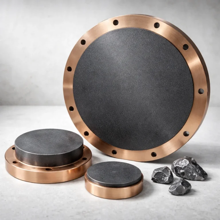
For more information about copper selenide sputtering targets, including available sizes and specifications, visit:
Copper Selenide Sputtering Targets (CuSe2) at AtoZmat
AtoZmat —— Advanced Materials from A to Z.
9. References
[1] Hussain, R. A.; Hussain, I. Copper Selenide Thin Films from Growth to Applications. Solid State Sciences 2020, 100, 106101. DOI: 10.1016/j.solidstatesciences.2019.106101
[2] Huang, X.-L.; Ao, D.-W.; Chen, T.-B.; Chen, Y.-X.; Li, F.; Chen, S.; Liang, G.-X.; Zhang, X.-H.; Zheng, Z.-H.; Fan, P. High-Performance Copper Selenide Thermoelectric Thin Films for Flexible Thermoelectric Application. Materials Today Energy 2021, 21, 100743. DOI: 10.1016/j.mtener.2021.100743
[3] Lin, Z.; Hollar, C.; Kang, J. S.; Yin, A.; Wang, Y.; Shiu, H.; Huang, Y.; Hu, Y.; Zhang, Y.; Duan, X. A Solution Processable High‐Performance Thermoelectric Copper Selenide Thin Film. Advanced Materials 2017, 29 (21). DOI: 10.1002/adma.201606662
[4] Fan, P.; Huang, X.; Chen, T.; Li, F.; Chen, Y.; Jabar, B.; Chen, S.; Ma, H.; Liang, G.; Luo, J.; Zhang, X.; Zheng, Z. α-Cu2Se Thermoelectric Thin Films Prepared by Copper Sputtering into Selenium Precursor Layers. Chemical Engineering Journal 2021, 410, 128444. DOI: 10.1016/j.cej.2021.128444
[5] Lv, Y.; Chen, J.; Zheng, R.-K.; Shi, X.; Song, J.; Zhang, T.; Li, X.; Chen, L. (001)-Oriented Cu2-ySe Thin Films with Tunable Thermoelectric Performances Grown by Pulsed Laser Deposition. Ceramics International 2015, 41 (6), 7439–7445. DOI: 10.1016/j.ceramint.2015.02.062
[6] Wu, Z.; Wu, J.; Li, Y.; Li, G. Effect of Cu Content on Electrical Properties of Evaporated Cu-Se Thermoelectric Films. Ceramics International 2020, 46 (13), 21617–21622. DOI: 10.1016/j.ceramint.2020.05.267
[7] Irfan, M.; Butt, S.; Sumayya; Akram, M. W.; Saadullah, M.; Basit, M. A.; Ahmad, J.; Yasir, M.; Ozair, H. Unlocking the Effect of Film Thickness on the Thermoelectric Properties of Thermally Evaporated Cu2−xSe Thin Films. RSC Advances 2024, 14 (51), 37688–37695. DOI: 10.1039/d4ra06908k
[8] Fan, P.; Huang, X.; Chen, T.; Li, F.; Chen, Y.; Jabar, B.; Chen, S.; Ma, H.; Liang, G.; Luo, J.; Zhang, X.; Zheng, Z. α-Cu2Se Thermoelectric Thin Films Prepared by Copper Sputtering into Selenium Precursor Layers. Chemical Engineering Journal 2021, 410, 128444. DOI: 10.1016/j.cej.2021.128444
[9] Forster, J. D.; Lynch, J. J.; Coates, N. E.; Liu, J.; Jang, H.; Zaia, E.; Gordon, M. P.; Szybowski, M.; Sahu, A.; Cahill, D. G.; Urban, J. J. Solution-Processed Cu2Se Nanocrystal Films with Bulk-Like Thermoelectric Performance. Scientific Reports 2017, 7 (1). DOI: 10.1038/s41598-017-02944-1
[10] Wu, Z.; Wu, J.; Li, Y.; Li, G. Effect of Cu Content on Electrical Properties of Evaporated Cu-Se Thermoelectric Films. Ceramics International 2020, 46 (13), 21617–21622. DOI: 10.1016/j.ceramint.2020.05.267
[11] Jackson, P.; Hariskos, D.; Lotter, E.; Paetel, S.; Wuerz, R.; Menner, R.; Wischmann, W.; Powalla, M. New World Record Efficiency for Cu(In,Ga)Se2 Thin‐film Solar Cells beyond 20%. Progress in Photovoltaics: Research and Applications 2011, 19 (7), 894–897. DOI: 10.1002/pip.1078
[12] Pallavolu, M. R.; Banerjee, A. N.; Minnam Reddy, V. R.; Joo, S. W.; Barai, H. R.; Park, C. Status Review on the Cu2SnSe3 (CTSe) Thin Films for Photovoltaic Applications. Solar Energy 2020, 208, 1001–1030. DOI: 10.1016/j.solener.2020.07.095
[13] Chen, N.; Scimeca, M. R.; Paul, S. J.; Hafiz, S. B.; Yang, Z.; Liu, X.; Yang, F.; Ko, D.-K.; Sahu, A. High-Performance Thermoelectric Silver Selenide Thin Films Cation Exchanged from a Copper Selenide Template. Nanoscale Advances 2020, 2 (2), 856–864. DOI: 10.1039/c9na00605b
[14] Xie, J.; Han, M.; Zeng, X.; Mao, D.; Li, H.; Zeng, X.; Liu, R.; Ren, L.; Sun, R.; Xu, J. Flexible pCu2Se-nAg2Se Thermoelectric Devices via in Situ Conversion from Printed Cu Patterns. Chemical Engineering Journal 2022, 435, 135172. DOI: 10.1016/j.cej.2022.135172
[15] Huang, X.-L.; Ao, D.-W.; Chen, T.-B.; Chen, Y.-X.; Li, F.; Chen, S.; Liang, G.-X.; Zhang, X.-H.; Zheng, Z.-H.; Fan, P. High-Performance Copper Selenide Thermoelectric Thin Films for Flexible Thermoelectric Application. Materials Today Energy 2021, 21, 100743. DOI: 10.1016/j.mtener.2021.100743
[16] Wu, Z.; Wu, J.; Li, Y.; Li, G. Effect of Cu Content on Electrical Properties of Evaporated Cu-Se Thermoelectric Films. Ceramics International 2020, 46 (13), 21617–21622. DOI: 10.1016/j.ceramint.2020.05.267
[17] Chen, N.; Scimeca, M. R.; Paul, S. J.; Hafiz, S. B.; Yang, Z.; Liu, X.; Yang, F.; Ko, D.-K.; Sahu, A. High-Performance Thermoelectric Silver Selenide Thin Films Cation Exchanged from a Copper Selenide Template. Nanoscale Advances 2020, 2 (2), 856–864. DOI: 10.1039/c9na00605b
[18] Xie, J.; Han, M.; Zeng, X.; Mao, D.; Li, H.; Zeng, X.; Liu, R.; Ren, L.; Sun, R.; Xu, J. Flexible pCu2Se-nAg2Se Thermoelectric Devices via in situ Conversion from Printed Cu Patterns. Chemical Engineering Journal 2022, 435, 135172. DOI: 10.1016/j.cej.2022.135172
[19] Chen, N.; Scimeca, M. R.; Paul, S. J.; Hafiz, S. B.; Yang, Z.; Liu, X.; Yang, F.; Ko, D.-K.; Sahu, A. High-Performance Thermoelectric Silver Selenide Thin Films Cation Exchanged from a Copper Selenide Template. Nanoscale Advances 2020, 2 (2), 856–864. DOI: 10.1039/c9na00605b
[20] Lin, Z.; Hollar, C.; Kang, J. S.; Yin, A.; Wang, Y.; Shiu, H.; Huang, Y.; Hu, Y.; Zhang, Y.; Duan, X. A Solution Processable High‐Performance Thermoelectric Copper Selenide Thin Film. Advanced Materials 2017, 29 (21). DOI: 10.1002/adma.201606662