Hafnium dioxide (HfO₂) has emerged as a critical material in modern semiconductor technology, serving as a high-k gate dielectric that enables continued scaling of complementary metal-oxide-semiconductor (CMOS) devices and facilitates the development of next-generation ferroelectric field-effect transistor (FeFET) memory devices. This article comprehensively reviews the properties, fabrication, and applications of HfO₂ sputtering targets, highlighting their role in depositing high-quality thin films for advanced semiconductor devices.
Quick Navigation
- What is Hafnium Dioxide (HfO₂)?
- Material Properties
- Sputtering Target Fabrication
- Deposition Techniques
- Applications in CMOS
- FeFET Memory Applications
- Manufacturing Considerations
- Future Perspectives
- FAQ
What is Hafnium Dioxide (HfO₂)?
Hafnium dioxide (HfO₂) represents a paradigm shift in semiconductor gate dielectric technology. As the relentless scaling of semiconductor devices drove the search for alternatives to silicon dioxide (SiO₂)—which reached physical limits below 2 nm due to excessive gate leakage currents [1]—hafnium-based oxides emerged as the leading solution.
HfO₂ serves as a high-k dielectric material (dielectric constant k ~ 25) that enables physically thicker films while maintaining equivalent electrical thickness compared to ultra-thin SiO₂. This property dramatically reduces gate leakage currents by several orders of magnitude, solving the tunneling crisis that threatened Moore’s Law progression.
Beyond conventional CMOS applications, HfO₂ has revealed ferroelectric properties when properly doped, opening entirely new applications in non-volatile memory technology (FeFETs).
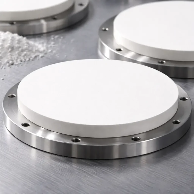
HfO₂ sputtering targets are the critical source materials for depositing these high-quality thin films via radio-frequency (RF) magnetron sputtering, offering excellent control over film composition, uniformity, and stoichiometry [2].
Material Properties
Key Physical and Electrical Characteristics
| Property | Value | Significance |
|---|---|---|
| Dielectric Constant (k) | ~25 (monoclinic: 16-20; tetragonal/cubic: 30-70) | Enables EOT scaling while maintaining physical thickness |
| Band Gap | 5.5–5.9 eV | Provides adequate barrier heights for electrons/holes |
| Crystallization Temperature | >400°C | Compatible with CMOS thermal budgets |
| Thermal Stability | Up to ~1000°C on Si | Prevents interface reactions during processing |
| Density | 9.68 g/cm³ (bulk) | Target density >95% theoretical required |
Crystal Structure and Phase Behavior
HfO₂ exists in three primary polymorphic forms:
- Monoclinic Phase (stable at room temperature): k ~ 16-20, P2₁/c symmetry
- Tetragonal Phase (stable >1700°C): k ~ 30-70, P4₂/nmc symmetry
- Cubic Phase (stable >2600°C): k ~ 30, Fm-3m symmetry
Phase Engineering: For CMOS applications, stabilization of higher-k phases (tetragonal/cubic) at room temperature is achieved through doping with Si, Al, or Zr, significantly enhancing dielectric properties [5].
Ferroelectric Properties (Doped HfO₂)
When doped with Si or Zr, HfO₂ exhibits robust ferroelectricity:
- Remanent Polarization (Pᵣ): 10–40 μC/cm²
- Coercive Field (E꜀): 1–2 MV/cm
- Endurance: >10¹⁰ cycles
- Retention: >10 years at 85°C [17,18]
Sputtering Target Fabrication
Manufacturing Process
High-quality HfO₂ sputtering targets require precise powder metallurgy processing:
Raw HfO₂ Powder (99.99%+)
    ↓
Milling & Particle Size Control
    ↓
Cold Isostatic Pressing (CIP)
    ↓
High-Temperature Sintering (1400–1600°C)
    ↓
Precision Machining
    ↓
Bonding to Backing Plate (Cu/Mo)
Critical Quality Specifications
| Parameter | Requirement | Test Method |
|---|---|---|
| Purity | ≥99.99% | ICP-MS |
| Density | >95% theoretical | Archimedes method |
| Grain Size | Uniform, <50 μm | SEM analysis |
| Stoichiometry | O/Hf ≈ 2.0 | XPS/GDMS |
| Bonding Integrity | Void-free, thermal resistance | Ultrasonic testing |
Specialized Target Types
- HfZrO₄ Targets: For ferroelectric memory applications (Zr:Hf ratio optimized for phase control)
- Si-doped HfO₂: Improved thermal stability and interface properties
- Al-doped HfO₂: Work function tuning in metal gate stacks [10]
Deposition Techniques
RF Magnetron Sputtering Parameters
| Process Parameter | Typical Range | Impact on Film Quality |
|---|---|---|
| RF Power | 100–300 W (4-inch target) | Deposition rate, ion damage |
| Process Pressure | 1–10 mTorr | Film density, stress |
| Gas Mixture | Ar or Ar/O₂ (2-10%) | Stoichiometry control |
| Substrate Temperature | RT – 300°C | Crystallinity, roughness |
| Post-Deposition Anneal | 400–600°C | Density, dielectric constant |
Film Characteristics
Sputtered HfO₂ films exhibit:
- Thickness Uniformity: <5% variation across 200 mm wafers
- Refractive Index: 1.9–2.1 (@ 632 nm)
- RMS Roughness: <1 nm for 10 nm films
- Density: 8.5–9.5 g/cm³ [12]
Interface Engineering
The HfO₂/Si interface quality critically affects device performance. Interfacial layers (SiO₂ or SiON, 0.5–1.0 nm) are intentionally incorporated to:
- Reduce interface state density (Dᵢₜ)
- Improve carrier mobility
- Control threshold voltage (Vₜₕ)
- Enhance reliability [13]
Applications in Advanced CMOS Technology
High-k Metal Gate (HKMG) Technology
Intel’s 45 nm process (2007) marked the first commercial implementation of HfO₂-based HKMG, achieving:
- 20% improvement in drive current (Iₒₙ)
- 10× reduction in gate leakage (I₉ₒff)
- 30% reduction in switching power [14]
Scaling Benefits
HfO₂ enables continued CMOS scaling through:
- Equivalent Oxide Thickness (EOT) Scaling: Achieving EOT <1 nm with acceptable leakage
- Mobility Enhancement: Through strain engineering and interface optimization
- Reliability Improvement: Reduced bias temperature instability (BTI) and time-dependent dielectric breakdown (TDDB) [15]
Integration Challenges
| Challenge | Solution Approach |
|---|---|
| Threshold Voltage Control | Metal gate work function engineering (TiN, TaN) |
| Mobility Degradation | Optimized interfacial layers, strain techniques |
| Fermi Level Pinning | Gate-last integration schemes |

Ferroelectric HfO₂ for FeFET Memory Devices
The Ferroelectric Discovery (2011)
The 2011 discovery of ferroelectricity in doped HfO₂ (specifically Si:HfO₂ and HfZrO₄) revolutionized non-volatile memory [6,7]. Unlike traditional perovskite ferroelectrics (PZT, SBT), HfO₂-based ferroelectrics are:
- CMOS compatible (no Pb contamination)
- Scalable to <10 nm thickness
- Process-compatible with standard thermal budgets
FeFET Device Architecture
Operating Principle:
- Write: Voltage pulse switches polarization (↑↓ domains)
- Read: Detect threshold voltage shift (ΔVₜₕ ≈ 0.5–1.0 V) due to polarization state
- Advantage: Non-destructive readout (unlike FeRAM)
Performance Metrics
| Characteristic | HfO₂-based FeFET | Conventional Flash |
|---|---|---|
| Write Voltage | 3–5 V | 10–15 V |
| Write Speed | <10 ns | μs–ms |
| Endurance | >10¹⁰ cycles | 10⁵–10⁶ cycles |
| Retention | >10 years | >10 years |
| Scalability | Sub-10 nm | Limited by tunnel oxide |
Manufacturing Considerations
Target Lifetime and Utilization
| Metric | Typical Value | Optimization Strategy |
|---|---|---|
| Erosion Rate | 0.1–0.3 μm/kWh | Power density control |
| Target Life | 500–2000 kWh | Uniform erosion design |
| Utilization Efficiency | 30–40% (planar) | Rotating cathode design |
Cost Structure
- Raw Material: Hfium is co-produced with zirconium; supply affects pricing
- Processing: High-temperature sintering (>1400°C) and precision diamond-grinding
- Recycling: Target reclaim programs recover 90%+ of hafnium value [22]
Quality Control Protocol
- Chemical Purity: ICP-MS for metallic impurities (<10 ppm total)
- Phase Analysis: XRD to confirm monoclinic phase stability
- Microstructure: SEM/EDS for grain boundary analysis
- Electrical Validation: Test deposition and C-V characterization
Future Perspectives
Emerging Applications
Beyond CMOS and memory, HfO₂ targets enable:
- Neuromorphic Computing: Ferroelectric synaptic devices for AI hardware
- Quantum Computing: High-k dielectrics for superconducting qubits
- Integrated Photonics: High-index contrast waveguides (n ~ 2.0 at 1550 nm)
- Energy Harvesting: Piezoelectric nanogenerators [24]
Technical Roadmap
Near-term (2024–2027):
- EOT scaling to <0.5 nm with molecular layer deposition (MLD) interfaces
- 3D NAND integration with ferroelectric HfO₂ charge-trap layers
Long-term (2028+):
- Negative capacitance FETs (NC-FETs) using ferroelectric HfO₂
- 2D channel integration (MoS₂, WS₂) with HfO₂ gate stacks [25]
Material Innovations
- Nanocomposite Targets: HfO₂-ZrO₂ gradient compositions for adaptive ferroelectricity
- Doped Targets: Precise La, Gd doping for negative capacitance applications
- Large-format Targets: 450 mm targets for next-gen fab tooling
FAQ
Q1: What is the dielectric constant of HfO₂ sputtered films? A: Typically 16–25 for amorphous/monoclinic phases, potentially 30–70 for stabilized tetragonal/cubic phases through doping or annealing.
Q2: Why did the industry choose HfO₂ over other high-k materials like ZrO₂ or Al₂O₃? A: HfO₂ offers the optimal combination of high k-value (25), wide bandgap (5.7 eV), and thermal stability with silicon. While ZrO₂ has higher k, it has poorer thermal stability; Al₂O₃ has lower k (9).
Q3: What causes ferroelectricity in doped HfO₂? A: Doping with Si, Zr, or Al stabilizes the non-centrosymmetric orthorhombic phase (Pca2₁), enabling switchable spontaneous polarization.
Q4: How thick can HfO₂ ferroelectric films be while maintaining polarization? A: Unlike traditional ferroelectrics that degrade below 50 nm, HfO₂ maintains ferroelectricity down to <5 nm, making it ideal for aggressively scaled FeFETs.
Q5: What is the typical deposition rate for HfO₂ sputtering? A: 5–20 nm/min depending on RF power (100–300 W), pressure, and target-to-substrate distance.
Q6: How does target density affect film quality? A: Low-density targets (<90%) cause arcing, particle generation, and nodule formation. High-density targets (>95%) ensure stable plasma and uniform film thickness.
Q7: Is HfO₂ compatible with gallium nitride (GaN) devices? A: Yes, HfO₂ is increasingly used as gate dielectric for GaN HEMTs (high-electron-mobility transistors) due to its wide bandgap and thermal stability.
Conclusion
HfO₂ sputtering targets have become indispensable in advanced semiconductor manufacturing, bridging the gap between fundamental materials science and commercial device fabrication. From enabling high-k metal gate CMOS scaling to unlocking ferroelectric memory applications, the quality of HfO₂ targets directly impacts device performance, yield, and reliability.
As the industry progresses toward sub-3 nm nodes and explores beyond-CMOS architectures including neuromorphic and quantum computing, the requirements for HfO₂ target purity, uniformity, and compositional control will become increasingly stringent. Continuous innovation in powder synthesis, sintering technologies, and target bonding methods will remain critical for meeting these future demands.
The transformation of HfO₂ from a simple high-k dielectric to a multifunctional ferroelectric material exemplifies how materials engineering continues to drive the expansion of Moore’s Law and the diversification of computing paradigms.
Product: Hafnium Oxide Sputtering Targets (HfO2 Sputtering Targets) | HfO2-ST
AtoZmat —— Advanced Materials from A to Z.
References
[1] Wilk, G. D.; Wallace, R. M.; Anthony, J. M. High-κ Gate Dielectrics: Current Status and Materials Properties Considerations. J. Appl. Phys. 2001, 89 (10), 5243–5275. DOI: 10.1063/1.1361065
[2] Robertson, J. High Dielectric Constant Gate Oxides for Metal Oxide Si Transistors. Rep. Prog. Phys. 2006, 69 (2), 327–396. DOI: 10.1088/0034-4885/69/2/R02
[3] Hubbard, K. J.; Schlom, D. G. Thermodynamic Stability of Binary Oxides in Contact with Silicon. J. Mater. Res. 1996, 11 (11), 2757–2776. DOI: 10.1557/JMR.1996.0350
[4] Gusev, E. P.; Cartier, E.; Buchanan, D. A.; Gribelyuk, M.; Copel, M.; Okorn-Schmidt, H.; D’Emic, C. Ultrathin High-K Metal Oxides on Silicon: Processing, Characterization and Integration Issues. Microelectron. Eng. 2001, 59 (1–4), 341–349. DOI: 10.1016/S0167-9317(01)00669-3
[5] Mistry, K.; Allen, C.; Auth, C.; Beattie, B.; Bergstrom, D.; Bost, M.; Brazier, M.; Buehler, M.; Cappellani, A.; Chau, R.; et al. A 45nm Logic Technology with High-k+Metal Gate Transistors, Strained Silicon, 9 Cu Interconnect Layers, 193nm Dry Patterning, and 100% Pb-free Packaging. Proc. IEEE Int. Electron Devices Meet. 2007, 247–250. DOI: 10.1109/IEDM.2007.4418914
[6] Böscke, T. S.; Müller, J.; Bräuhaus, D.; Schröder, U.; Böttger, U. Ferroelectricity in Hafnium Oxide Thin Films. Appl. Phys. Lett. 2011, 99 (10), 102903. DOI: 10.1063/1.3634052
[7] Müller, J.; Böscke, T. S.; Schröder, U.; Mueller, S.; Bräuhaus, D.; Böttger, U.; Frey, L.; Mikolajick, T. Ferroelectricity in Simple Binary ZrO₂ and HfO₂. Nano Lett. 2012, 12 (8), 4318–4323. DOI: 10.1021/nl302049k
[8] Park, M. H.; Lee, Y. H.; Kim, H. J.; Schenk, T.; Lee, W.; Kim, K. D.; Fengler, F. P. G.; Schroeder, U.; Mikolajick, T.; Hwang, C. S. Surface and Grain Boundary Scavenging in HfO₂-Based Ferroelectric Thin Films. Adv. Electron. Mater. 2017, 3 (12), 1700489. DOI: 10.1002/aelm.201700489
[9] Hoffmann, M.; Pesic, M.; Chatterjee, K.; Khan, A. I.; Salahuddin, S.; Slesazeck, S.; Schroeder, U.; Mikolajick, T. Direct Correlation of Ferroelectric Properties and Memory Characteristics in Ferroelectric Tunnel Junctions. IEEE J. Electron Devices Soc. 2016, 4 (4), 192–200. DOI: 10.1109/JEDS.2016.2560219
[10] Florent, K.; Lavizzari, S.; Popovici, M.; Di Piazza, L.; Arreghini, A.; Degraeve, R.; Groeseneken, G.; Van Houdt, J. Understanding the Switching and Reliability of HfO₂-Based Ferroelectric Memories Through a Kinetic Model for Ferroelectric Switching. IEEE Trans. Electron Devices 2018, 65 (6), 2387–2393. DOI: 10.1109/TED.2018.2829122
[11] Ali, T.; Polakowski, P.; Riedel, S.; Büttner, T.; Kämpfe, T.; Rudolph, M.; Pätzold, B.; Seidel, K.; Löhr, D.; Hoffmann, R.; et al. Silicon Doped Hafnium Oxide (HSO) and Hafnium Zirconium Oxide (HZO) Based FeFET: A Material Relation to Device Physics. Appl. Phys. Lett. 2018, 112 (22), 222903. DOI: 10.1063/1.5029324
[12] Mikolajick, T.; Slesazeck, S.; Park, M. H.; Schroeder, U. Ferroelectric Hafnium Oxide for Ferroelectric Random-Access Memories and Ferroelectric Field-Effect Transistors. MRS Bull. 2018, 43 (5), 340–346. DOI: 10.1557/mrs.2018.92
[13] Müller, J.; Yurchuk, E.; Schlösser, T.; Paul, J.; Hoffmann, R.; Müller, S.; Martin, D.; Slesazeck, S.; Polakowski, P.; Sundqvist, J.; et al. Ferroelectricity in HfO₂ Enables Nonvolatile Data Storage in 28 nm HKMG. Proc. IEEE Symp. VLSI Technol. 2012, 25–26. DOI: 10.1109/VLSIT.2012.6242444
[14] Schroeder, U.; Yurchuk, E.; Müller, J.; Martin, D.; Schenk, T.; Polakowski, P.; Adelmann, C.; Kalinin, A.; Popovici, M.; Persson, K. M.; et al. Impact of Different Dopants on the Switching Properties of Ferroelectric Hafniumoxide. Jpn. J. Appl. Phys. 2014, 53 (8S1), 08LE02. DOI: 10.7567/JJAP.53.08LE02
[15] Park, M. H.; Lee, Y. H.; Kim, H. J.; Kim, Y. J.; Moon, T.; Kim, K. D.; Müller, J.; Kersch, A.; Schroeder, U.; Mikolajick, T.; Hwang, C. S. Ferroelectricity and Antiferroelectricity of Doped Thin HfO₂-Based Films. Adv. Mater. 2015, 27 (11), 1811–1831. DOI: 10.1002/adma.201404531
[16] Kim, S. J.; Mohan, J.; Summerfelt, S. R.; Kim, J. Ferroelectric Hf₀.₅Zr₀.₅O₂ Thin Films: A Review of Recent Advances. JOM 2019, 71 (1), 246–255. DOI: 10.1007/s11837-018-3140-5