The discovery of ferroelectricity in doped hafnium oxide (HfO₂) has revolutionized the field of non-volatile memory technology, offering a CMOS-compatible solution that overcomes the scaling limitations of traditional perovskite-based ferroelectrics. This article explores the development and application of HfPrO (hafnium-praseodymium oxide) sputtering targets for the deposition of ferroelectric thin films.
We examine:
- The materials science behind rare-earth doping of hafnia
- The fabrication of ceramic sputtering targets
- Deposition techniques and process optimization
- Integration into next-generation memory devices including FeRAMs (Ferroelectric Random Access Memories) and FeFETs (Ferroelectric Field-Effect Transistors)
The unique properties of praseodymium-doped hafnia films, their compatibility with existing semiconductor manufacturing processes, and their potential for neuromorphic computing applications are discussed in detail.
What’s Driving Next-Generation Ferroelectric Memory?
The relentless pursuit of higher density, faster, and more energy-efficient non-volatile memory has led researchers to explore novel materials beyond conventional flash memory technology. Ferroelectric materials have long been considered promising candidates due to their bistable polarization states that can be switched by an external electric field [1].
However, traditional perovskite ferroelectrics such as Pb(Zr,Ti)O₃ (PZT) and SrBi₂Ta₂O₉ (SBT) face significant challenges in scaling and integration with complementary metal-oxide-semiconductor (CMOS) processes [2].
The Hafnia Breakthrough
The breakthrough discovery of ferroelectricity in silicon-doped hafnium oxide (Si:HfO₂) in 2011 opened new avenues for ferroelectric memory technology [2]. Hafnium oxide offers a decisive advantage: it is already a standard material in CMOS processes as a high-k dielectric, making it inherently compatible with existing semiconductor manufacturing.
Subsequent research has revealed that various dopants, including rare-earth elements like yttrium, gadolinium, and praseodymium, can stabilize the ferroelectric orthorhombic phase in HfO₂ [1].
Materials Science of Ferroelectric Hafnia
Phase Stabilization in Doped HfO₂
Hafnium oxide naturally crystallizes in the monoclinic phase at room temperature, which is centrosymmetric and non-ferroelectric. The ferroelectric properties emerge when the material is stabilized in the orthorhombic phase (space group Pca2₁) [1].
This stabilization can be achieved through several mechanisms:
- Doping: Introduction of aliovalent cations such as Si⁴⁺, Al³⁺, Y³⁺, Gd³⁺, or Pr³⁺ creates oxygen vacancies and induces lattice strain that favors the orthorhombic phase [1].
- Confinement effects: Thin films constrained between electrodes experience mechanical stress that can stabilize non-equilibrium phases [3].
- Surface energy effects: The increased surface-to-volume ratio in ultrathin films influences phase stability [1].
Why Praseodymium? Praseodymium doping is particularly interesting due to the ionic radius of Pr³⁺ (1.13 Å) and Pr⁴⁺ (0.96 Å), which creates significant lattice distortion when substituting for Hf⁴⁺ (0.83 Å). This size mismatch introduces substantial strain that promotes the formation of the ferroelectric orthorhombic phase [1].
HfPrO Composition Optimization
The optimal praseodymium concentration in HfPrO films typically ranges from 2-6 atomic percent. Higher doping levels may lead to phase separation or the formation of non-ferroelectric phases. The exact composition depends on:
- Deposition method
- Thermal budget
- Electrode materials [1]
Research has shown that rare-earth dopants not only stabilize the ferroelectric phase but also influence key properties such as coercive field, remanent polarization, and endurance characteristics [1].
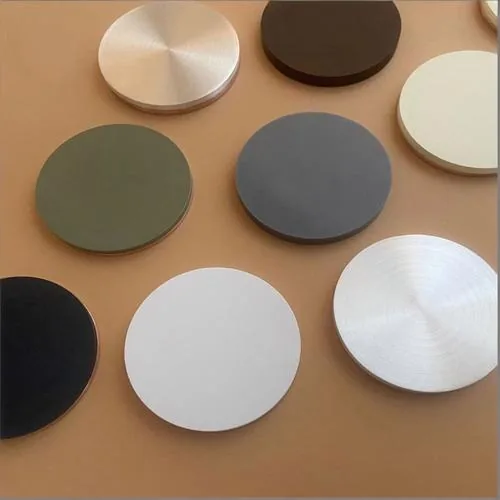
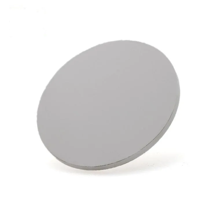
Sputtering Target Fabrication
Ceramic Target Manufacturing
The production of high-quality HfPrO sputtering targets requires specialized ceramic processing techniques. The manufacturing process typically involves several key steps [4]:
1. Powder Preparation High-purity hafnium oxide (HfO₂) and praseodymium oxide (Pr₆O₁₁) powders are mixed in the desired stoichiometric ratio. The powders must have controlled particle size distribution and high chemical purity to ensure uniform composition in the final target.
2. Milling and Mixing The powder mixture undergoes ball milling to achieve homogeneous distribution and reduce particle size, which improves sintering behavior.
3. Forming The mixed powder is formed into green bodies using techniques such as:
- Uniaxial pressing
- Cold isostatic pressing (CIP)
- Slip casting for complex geometries
4. Sintering The green bodies are sintered at high temperatures (typically 1400-1600°C) to achieve near-theoretical density. The sintering atmosphere must be carefully controlled to maintain the desired oxygen stoichiometry.
5. Hot Isostatic Pressing (HIP) Optional HIP treatment can further increase density and eliminate residual porosity, which is crucial for preventing arcing during sputtering.
6. Machining and Bonding The sintered ceramic is machined to final dimensions and bonded to a metallic backing plate (typically copper or aluminum) using specialized bonding techniques such as soldering or diffusion bonding [4].
Quality Control Parameters
Critical quality parameters for HfPrO sputtering targets include:
| Parameter | Specification |
|---|---|
| Density | >95% of theoretical density |
| Chemical homogeneity | Uniform distribution of praseodymium throughout the target |
| Microstructure | Fine-grained, uniform microstructure |
| Purity | Minimal metallic impurities (<100 ppm) |
| Mechanical integrity | High fracture toughness to withstand thermal stresses during sputtering [4] |
Thin Film Deposition Techniques
Reactive Sputtering from HfPrO Targets
Reactive magnetron sputtering using HfPrO ceramic targets offers several advantages for ferroelectric thin film deposition:
- Composition control: The fixed composition of the ceramic target ensures reproducible film stoichiometry, unlike co-sputtering from separate metal targets [4].
- Process stability: Ceramic targets enable stable sputtering in inert atmospheres, avoiding the complexities of reactive sputtering from metallic targets [4].
- Uniformity: Modern magnetron designs with rotating targets provide excellent thickness uniformity over large substrate areas.
Optimized Sputtering Process Parameters:
| Parameter | Typical Range |
|---|---|
| Power density | 2-5 W/cm² (RF sputtering) |
| Pressure | 1-10 mTorr argon atmosphere |
| Substrate temperature | 200-400°C during deposition |
| Post-deposition annealing | Rapid thermal annealing (RTA) at 400-600°C in nitrogen or forming gas to crystallize the ferroelectric phase [1] |
Alternative Deposition Methods
While sputtering is the focus of this article, other deposition methods have also been employed for ferroelectric hafnia films:
- Atomic layer deposition (ALD): Excellent conformality and thickness control
- Chemical solution deposition (CSD): Low-cost, suitable for research
- Pulsed laser deposition (PLD): High-quality epitaxial films [1]
Device Integration and Memory Applications
Ferroelectric Random Access Memory (FeRAM)
FeRAM devices store information in the polarization state of a ferroelectric capacitor. The 1T-1C (one transistor, one capacitor) FeRAM cell structure benefits significantly from HfPrO films due to [2]:
- Scalability: HfPrO films maintain ferroelectric properties down to thicknesses below 10 nm, enabling continued scaling beyond the limits of perovskite ferroelectrics [2].
- CMOS compatibility: Hafnium oxide is already integrated in CMOS processes as a high-k gate dielectric, simplifying integration [2].
- Three-dimensional integration: The conformal deposition capability of sputtered HfPrO films enables 3D capacitor structures for increased density [5].
Ferroelectric Field-Effect Transistors (FeFETs)
FeFETs incorporate the ferroelectric layer directly into the gate stack of a MOSFET, creating a memory transistor. HfPrO offers advantages for FeFET applications [2]:
- Low permittivity: The relatively low dielectric constant (~30) of ferroelectric hafnia compared to perovskites (>100) provides better voltage coupling to the channel [2].
- High coercive field: The higher coercive field of HfPrO (~1-2 MV/cm) enables faster switching and better retention, though it presents challenges for endurance [2].
- Gate-first integration: HfPrO can withstand the thermal budget of gate-first CMOS processes [5].
Emerging Applications
Beyond conventional memory, HfPrO-based devices are finding applications in:
Neuromorphic Computing Ferroelectric memcapacitors based on HfPrO enable energy-efficient synaptic weight storage for artificial neural networks [6].
Ferroelectric Tunnel Junctions (FTJs) Ultrathin HfPrO layers can modulate tunnel current based on polarization state, enabling novel memory and logic devices [7].
In-Memory Computing The non-volatile nature of ferroelectric polarization enables computation within memory arrays, reducing data movement energy [5].
Performance Characteristics and Optimization
Electrical Properties
HfPrO thin films typically exhibit the following electrical characteristics when optimally processed [1]:
| Property | Typical Value |
|---|---|
| Remanent polarization (Pᵣ) | 10-30 μC/cm² |
| Coercive field (E꜀) | 1-2 MV/cm |
| Dielectric constant | 25-35 |
| Breakdown field | >4 MV/cm |
| Endurance | 10⁴-10¹⁰ cycles depending on film quality and electrode materials |
Reliability Considerations
Key reliability challenges for HfPrO-based memories include:
Wake-up Effect The initial increase in polarization with cycling, attributed to field-induced redistribution of defects [1].
Fatigue Gradual degradation of polarization with cycling, influenced by electrode interfaces and oxygen vacancy dynamics [1].
Retention Data retention at elevated temperatures, which depends on depolarization field and leakage current [2].
Imprint Asymmetric switching characteristics that develop over time [1].
Note: Interface engineering through appropriate electrode materials (TiN, TaN, W) and careful control of oxygen stoichiometry during deposition and annealing are critical for optimizing reliability [3].
Future Perspectives and Challenges
Scaling Roadmap
The continued scaling of HfPrO-based memories faces several challenges:
- Thickness scaling: Maintaining ferroelectric properties below 5 nm thickness
- 3D integration: Developing processes for high-aspect-ratio structures
- Multi-level cells: Achieving multiple distinct polarization states for increased density [5]
Materials Innovation
Future research directions include:
- Composition engineering: Exploring ternary and quaternary doping schemes for optimized properties
- Strain engineering: Using substrate-induced strain to enhance ferroelectricity [3]
- Interface optimization: Developing novel electrode materials with improved interface properties [3]
Manufacturing Integration
The transition from research to manufacturing requires:
- Process standardization: Establishing industry-standard deposition and annealing recipes
- Metrology development: Creating reliable characterization methods for production control
- Design-technology co-optimization: Developing circuit designs that leverage the unique properties of HfPrO memories [5]
Conclusion
HfPrO sputtering targets represent a critical enabling technology for the next generation of non-volatile memories based on ferroelectric hafnia. The combination of CMOS compatibility, scalability, and excellent ferroelectric properties positions HfPrO thin films as a leading candidate for future memory technologies.
Continued advances in target fabrication, deposition processes, and device integration will drive the commercialization of these materials, enabling energy-efficient computing from edge devices to data centers. As research progresses, HfPrO-based devices are poised to play a transformative role not only in memory but also in neuromorphic computing and in-memory processing architectures [6].
References
[1] Starschich, S.; Boettger, U. An Extensive Study of the Influence of Dopants on the Ferroelectric Properties of HfO₂. Journal of Materials Chemistry C 2017, 5 (2), 333–338. DOI: 10.1039/c6tc04807b
[2] Mikolajick, T.; Slesazeck, S.; Park, M. H.; Schroeder, U. Ferroelectric Hafnium Oxide for Ferroelectric Random-Access Memories and Ferroelectric Field-Effect Transistors. MRS Bulletin 2018, 43 (5), 340–346. DOI: 10.1557/mrs.2018.92
[3] Shi, S.; Xi, H.; Cao, T.; et al. Interface-Engineered Ferroelectricity of Epitaxial Hf₀.₅Zr₀.₅O₂ Thin Films. Nature Communications 2023, 14 (1). DOI: 10.1038/s41467-023-37560-3
[4] Simons, C.; Kastner, A.; Kiriakidis, G. Ceramic Target Materials for Sputtering Applications. Materials Science Forum 2010, 638–642, 805–811. DOI: 10.4028/www.scientific.net/msf.638-642.805
[5] Mikolajick, T.; Schroeder, U.; Lomenzo, P. D.; et al. Next Generation Ferroelectric Memories Enabled by Hafnium Oxide. In 2019 IEEE International Electron Devices Meeting (IEDM); IEEE, 2019; p 15.5.1-15.5.4. DOI: 10.1109/iedm19573.2019.8993447
[6] Wang, X.; Ye, S.; Cui, B.; et al. Hafnium Oxide-Based Nonvolatile Ferroelectric Memcapacitor Array for High Energy-Efficiency Neuromorphic Computing. Nano Energy 2025, 140, 111011. DOI: 10.1016/j.nanoen.2025.111011
[7] Lim, E.; Kim, D.; Park, J.; et al. Recent Advances in the Mechanism, Properties, and Applications of Hafnia Ferroelectric Tunnel Junctions. Journal of Physics D: Applied Physics 2024, 57 (38). DOI: 10.1088/1361-6463/ad7036