Silver‑tungsten (AgW) composites occupy a critical niche in electrical engineering by merging the outstanding electrical/thermal conductivity of silver with the high‑melting, hard, arc‑erosion‑resistant nature of tungsten. This review examines the fundamental science and engineering of AgW materials, focusing on three tightly linked application domains: (1) AgW sputtering targets for thin‑film deposition, (2) electrical contact materials for switching devices and circuit breakers, and (3) coatings for micro‑arc electrical‑discharge‑machining (EDM) electrodes. The processing‑microstructure‑property relationships, degradation mechanisms under arcing, and recent advances in manufacturing—including powder metallurgy, spark‑plasma sintering, and electro‑explosive deposition—are systematically presented.
1. What is the AgW Sputtering Target?
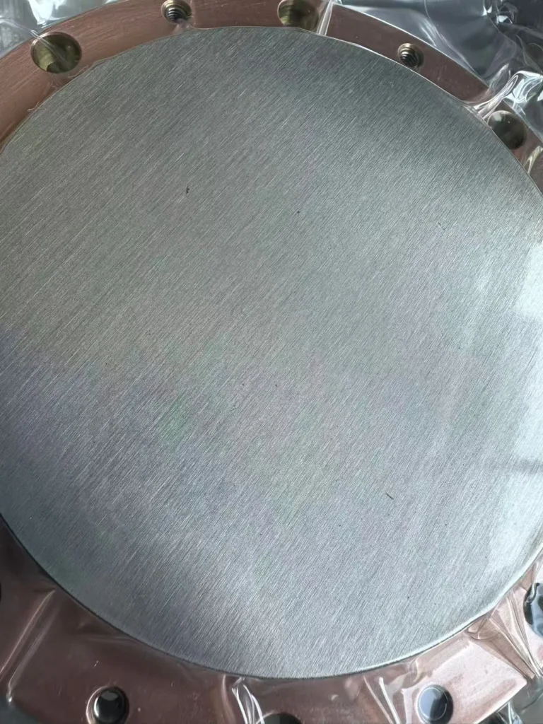
The AgW sputtering target is a composite material consisting of silver (Ag) and tungsten (W) that is used as a source in physical‑vapor‑deposition (PVD) processes to deposit thin Ag‑W films. The unique combination of Ag’s high electrical conductivity (≈ 63 × 10⁶ S m⁻¹) and thermal conductivity (≈ 429 W m⁻¹ K⁻¹) with W’s exceptional melting point (3422 °C), hardness, and resistance to arc erosion makes AgW ideal for high‑reliability electrical contacts and advanced electrode coatings.
Why it matters
- Electrical contacts in low‑voltage circuit breakers, contactors, relays, and switchgear rely on AgW to resist welding, material transfer, and erosion under arcing.
- Thin‑film applications in microelectronics and micro‑electromechanical systems (MEMS) benefit from Ag‑W films that act as diffusion barriers, contact metallizations, and stable electrodes.
- Micro‑EDM electrodes coated with AgW exhibit dramatically reduced wear and improved machining precision because the silver phase dissipates heat while the tungsten skeleton provides mechanical stability.
The following sections detail how AgW materials are processed, how their microstructure governs performance, and what emerging technologies are shaping the next generation of AgW‑based components.
2. Processing of AgW Sputtering Targets & Composite Materials
| Method | Key Steps | Typical Characteristics | Ref. |
|---|---|---|---|
| Press‑Sinter (PS) | Blend Ag + W powders → compact → sinter above Ag melting point (≈ 962 °C) | Liquid‑phase sintering; moderate density (≈ 90 % TD) | [6] |
| Press‑Sinter‑Infiltrate (PSI) | Sinter porous W preform → infiltrate with molten Ag | Near‑theoretical density; better homogeneity, lower residual porosity | [6] |
| Spark‑Plasma Sintering (SPS) | Rapid heating (≈ 100 °C min⁻¹) + high‑current pulsed DC, short dwell (≈ 5 min) | Fine microstructure, minimal grain growth, excellent density (> 99 % TD) | [7] |
| Electro‑Explosive Deposition (EED) | Electrical explosion of Ag/W conductors → high‑velocity plasma jet → coating | Ultra‑fine composite coating, strong adhesion, low heat‑affected zone | [5] |
2.1 Powder Metallurgy Routes
- Press‑Sinter (PS): Mixed Ag and W powders are pressed and sintered. The liquid silver phase wets the tungsten particles, forming a network. Density and properties depend on particle‑size distribution and sintering temperature.
- Press‑Sinter‑Infiltrate (PSI): A porous W skeleton is first produced, then molten Ag infiltrates the interconnected pores by capillary action. The resulting composite shows higher density and superior contact‑life performance compared with PS, even when composition and particle size are identical.
Key finding: For identical Ag content and W particle size, PSI yields lower contact resistance and longer service life, although oxidation behavior at 600–700 °C differs markedly (oxide morphology changes) [6].
2.2 Spark Plasma Sintering (SPS)
SPS enables rapid densification of Ag‑WC (or Ag‑W) composites while preserving a fine microstructure. The fast heating rates suppress excessive grain growth and interfacial reactions, producing contacts with stable contact resistance and enhanced arc‑erosion resistance. WC particle size strongly influences switching performance: finer WC reduces both contact resistance and its fluctuation [7].
2.3 AgW50 Composites
Osadnik et al. investigated AgW50 (50 wt % Ag, 50 wt % W) targeted for electric contacts. They demonstrated that starting tungsten powder particle‑size distribution and sintering parameters are decisive for achieving near‑theoretical density, high conductivity, and required hardness. Optimized processing yields composites with excellent electrical performance [8].
3. AgW in Electrical Contact Applications
3.1 Arc‑Erosion Mechanisms
- Arc formation during contact separation melts, vaporizes, and ejects material from the contact surface.
- Erosion rate is a function of arc current, silver content, and material density.
- Contacts with density close to 100 % TD exhibit lower erosion.
- Erosion rises gradually between 5–16 kA peak, then stabilizes at higher currents.
- Material transfer & welding are mitigated by the refractory W skeleton, which remains after Ag is displaced, preserving a conductive framework [9][10].
3.2 Role of Silver Content & Microstructure
| Ag (wt %) | Conductivity (×10⁶ S m⁻¹) | Hardness (HV) | Erosion Resistance |
|---|---|---|---|
| 30 | ≈ 30 | ≈ 200 | Moderate |
| 50 | ≈ 50 | ≈ 150 | Good |
| 70 | ≈ 60 | ≈ 100 | Lower |
- Even a small addition of W (≈ 5 wt %) dramatically reduces erosion while maintaining low contact resistance. The W particles act as a rigid framework that pins the Ag matrix, preventing large‑scale displacement during arcing [11][12].
- Fine WC particles improve thermal conductivity, aiding heat dissipation and reducing contact‑resistance drift [13].
3.3 Additive Effects
- Nickel (Ni) addition (1–10 wt %) to Ag‑WC (60‑40 wt %) gradually raises mean contact resistance from ≈ 2 mΩ to ≈ 3 mΩ. However, at higher Ni (≈ 10 wt %) a Ag‑rich surface layer forms during thermal cycling, dropping resistance to ≈ 1.5 mΩ due to improved wetting and Ag migration [14].
3.4 Oxidation & Corrosion
- Below 600 °C: oxidation rate modest; mainly Ag₂WO₄ forms.
- At 700 °C: oxidation rate jumps > 10×; WO₃ dominates, creating a porous oxide layer that dramatically raises contact resistance.
- The absence of a continuous Ag layer (removed by arcing) exposes the W skeleton, leading to high‑resistance tungsten oxides [1][6].
4. AgW Sputtering Targets for Thin‑Film Deposition
4.1 Magnetron Sputtering of Ag‑W Films
- Target requirements: uniform phase distribution, high density, mechanical integrity to survive sputtering stresses.
- Film properties: Ag‑W films with 2–3 at % W show improved thermal stability, reduced agglomeration, and better adhesion compared with pure Ag. Tungsten suppresses Ag diffusion and clustering, critical for high‑temperature interconnects [3].
4.2 Electroless Deposition of Ag‑W Films
- Process: Electroless plating from a solution containing Ag⁺ and WO₄²⁻ yields Ag‑W films (≈ 2–3 at % W).
- Benefits: Codeposited W atoms inhibit electromigration and agglomeration, producing lower resistivity than pure Ag of comparable thickness. These films are attractive for interconnect and contact metallization [4].
- W‑doped Ag films on p‑Si(100) (≈ 2.3 mol % W, O ≈ 4 mol %) exhibit good oxidation resistance at 350 °C, attributed to a thin protective W‑oxide layer [15].
4.3 Sputter Deposition of Multilayer Structures
- WO₃/Ag/WO₃ multilayers deposited by reactive sputtering serve as ITO‑free transparent electrodes for electrochromic devices. The thin Ag layer (10–20 nm) provides conductivity while WO₃ acts as the electrochromic layer. Uniformity and continuity of the Ag layer are crucial; doping with W or optimizing deposition parameters improves performance [16].
5. AgW Coatings for Micro‑Arc EDM Electrode Applications
5.1 Electro‑Explosive Deposition (EED)
- Method: An electrical explosion of Ag/W conductors creates a high‑velocity plasma jet that deposits a composite coating onto a substrate.
- Resulting coating: Fine W particles uniformly dispersed in an Ag matrix, with strong adhesion and a low heat‑affected zone.
- Performance: Under identical arc‑discharge conditions, EED‑coated contacts exhibit 2–3× lower erosion rates compared with uncoated Cu contacts [5].
5.2 Application to Micro‑EDM Electrodes
Micro‑EDM erodes conductive workpieces by discrete electrical discharges. AgW‑coated electrodes (typically on Cu or brass substrates) offer:
| Advantage | Mechanism |
|---|---|
| Higher tool life | Silver’s thermal conductivity dissipates spark heat; tungsten skeleton resists erosion. |
| Improved dimensional accuracy | Reduced electrode‑material transfer to the workpiece. |
| Better surface finish | Stable composite surface minimizes material redeposition. |
These benefits make AgW a promising coating for precision machining of hard materials (e.g., tungsten carbide, ceramics) [17].
5.3 Electro‑Spark Deposition (ESD)
- Process: Short‑duration, high‑current pulses melt AgW (or feed Ag onto a W electrode) and transfer it to the substrate.
- Coating characteristics: Strong metallurgical bond, low dilution, minimal heat‑affected zone.
- Result: Up to 50 % reduction in electrode wear during micro‑EDM of tungsten carbide [18].
6. Performance Characteristics & Degradation Mechanisms
6.1 Contact‑Resistance Behavior
- Contact resistance rises during switching due to oxide formation (WO₃) and loss of surface Ag.
- The density of the composite is crucial: higher density (lower porosity) yields more stable resistance because pores act as stress concentrators and crack pathways [19].
6.2 Erosion Resistance
- The refractory W skeleton remains after molten Ag is expelled, preserving a conductive network.
- Erosion rate increases with arc current up to a saturation point, beyond which it stabilizes.
- Porosity directly correlates with higher erosion; achieving > 99 % TD is desirable [9].
6.3 Welding Resistance
- Tungsten particles interrupt the continuity of molten Ag, reducing the contact area prone to welding.
- W also increases the viscosity of the molten pool, further inhibiting solidification welding [1][12].
7. Recent Advances & Future Directions
| Research Area | Key Development | Potential Impact |
|---|---|---|
| Nanostructured AgW | Use of nanocrystalline W powders and rapid SPS consolidation; grain‑growth suppression. | Enhanced hardness, finer refractory phase distribution, improved erosion resistance. |
| Graphene‑Enhanced AgW | Incorporation of graphene (≈ 0.1–0.5 wt %) as an extra conductive pathway and solid lubricant. | Lower contact resistance, reduced friction, better arc erosion performance. |
| Advanced Coating Technologies | High‑power impulse magnetron sputtering (HiPIMS) and atmospheric plasma spraying. | Tailored microstructure, controlled porosity, superior adhesion for both contacts and EDM electrodes. |
Emerging strategies aim to combine nanostructure, additive doping, and novel deposition methods to push the limits of conductivity, wear resistance, and thermal stability in AgW systems.
8. Conclusions
Silver‑tungsten (AgW) composites are a mature yet continually evolving class of functional materials essential for:
- Sputtering targets delivering thin Ag‑W films with superior thermal stability and electromigration resistance.
- Electrical contacts that resist arc erosion, welding, and oxidation in power‑distribution and switching devices.
- Micro‑EDM electrode coatings that dramatically extend tool life and machining precision.
The performance of AgW is intimately tied to processing: powder‑metallurgy routes (press‑sinter, press‑sinter‑infiltrate) and spark‑plasma sintering each offer distinct microstructural benefits, while emerging techniques such as electro‑explosive deposition and HiPIMS promise finer control over phase distribution and coating quality.
Future research will likely focus on nanostructured composites, graphene or other 2D additive enhancements, and advanced deposition technologies to meet the ever‑increasing demands of high‑current switching and precision manufacturing.
References
- M. T. Kesim, H. Yu, Y. Sun, M. Aindow, and S. P. Alpay, “Corrosion, oxidation, erosion and performance of Ag/W‑based circuit breaker contacts: A review,” Corrosion Science, vol. 135, pp. 12–34, May 2018. DOI: 10.1016/j.corsci.2018.02.010
- F. Findik and H. Uzun, “Microstructure, hardness and electrical properties of silver‑based refractory contact materials,” Materials & Design, vol. 24, no. 7, pp. 489–492, Oct. 2003. DOI: 10.1016/s0261‑3069(03)00125‑0
- A. Inberg, E. Ginsburg, Y. Shacham‑Diamand, N. Croitoru, and A. Seidman, “Electroless and sputtered silver–tungsten thin films for microelectronics applications,” Microelectronic Engineering, vol. 65, no. 1–2, pp. 197–207, Jan. 2003. DOI: 10.1016/s0167‑9317(02)00851‑1
- A. Inberg, Y. Shacham‑Diamand, E. Rabinovich, G. Golan, and N. Croitoru, “Electroless‑deposited Ag–W films for microelectronics applications,” Thin Solid Films, vol. 389, no. 1–2, pp. 213–218, Jun. 2001. DOI: 10.1016/s0040‑6090(01)00862‑8
- D. A. Romanov, S. V. Moskovsky, V. E. Gromov, and K. V. Sosnin, “Electroexplosive electrical erosion resistant coatings of the Ag‑W system used for electrical contacts of power mine equipment,” IOP Conference Series: Earth and Environmental Science, vol. 206, p. 012030, Nov. 2018. DOI: 10.1088/1755‑1315/206/1/012030
- C.-H. Leung, R. Bevington, P. Wingert, and H. Kim, “Effects of processing methods on the contact performance parameters for silver‑tungsten composite materials,” IEEE Trans. Compon., Hybrids, Manuf. Technol., vol. 5, no. 1, pp. 23–31, Mar. 1982. DOI: 10.1109/tchmt.1982.1135948
- N. Ray et al., “Novel processing of Ag‑WC electrical contact materials using spark plasma sintering,” Materials & Design, vol. 121, pp. 262–271, May 2017. DOI: 10.1016/j.matdes.2017.02.070
- M. Osadnik, M. Czepelak, and M. Kamińska, “Production and properties of AgW50 composites designated for electric contacts,” Key Eng. Mater., vol. 641, pp. 93–98, Apr. 2015. DOI: 10.4028/www.scientific.net/kem.641.93
- J. J. Shea, “Erosion and resistance characteristics of AgW and AgC contacts,” IEEE Trans. Compon. Packag. Technol., vol. 22, no. 2, pp. 331–336, Jun. 1999. DOI: 10.1109/6144.774755
- M. Lindmayer and M. Roth, “Contact resistance and arc erosion of W/Ag and WC/Ag,” IEEE Trans. Compon., Hybrids, Manuf. Technol., vol. 2, no. 1, pp. 70–75, Mar. 1979. DOI: 10.1109/tchmt.1979.1135414
- F. Holmes and P. Slade, “The erosion characteristics of Ag contacts and the effect of adding a small percentage of W,” IEEE Trans. Parts, Hybrids, Packag., vol. 13, no. 1, pp. 23–30, Mar. 1977. DOI: 10.1109/tphp.1977.1135177
- C.-H. Leung and H. Kim, “A comparison of Ag/W, Ag/WC, and Ag/Mo electrical contacts,” IEEE Trans. Compon., Hybrids, Manuf. Technol., vol. 7, no. 1, pp. 69–75, Mar. 1984. DOI: 10.1109/tchmt.1984.1136333
- N. Ray et al., “Effect of WC particle size and Ag volume fraction on electrical contact resistance and thermal conductivity of Ag–WC contact materials,” Materials & Design, vol. 85, pp. 412–422, Nov. 2015. DOI: 10.1016/j.matdes.2015.07.006
- N. Ray et al., “Effect of Ni addition on the contact resistance of Ag‑WC electrical contacts,” J. Alloys Compd., vol. 670, pp. 188–197, Jun. 2016. DOI: 10.1016/j.jallcom.2016.02.037
- W. Ye, C. Ma, C. Wang, and F. Zhou, “Electroless deposition of W‑doped Ag films onto p‑Si(100) from diluted HF solution,” Trans. Nonferrous Met. Soc. China, vol. 19, no. 6, pp. 1474–1478, Dec. 2009. DOI: 10.1016/s1003‑6326(09)60054‑6
- A. I. Inamdar et al., “Reactive sputter deposition of WO₃/Ag/WO₃ film for indium tin oxide (ITO)‑free electrochromic devices,” ACS Appl. Mater. Interfaces, vol. 8, no. 6, pp. 3964–3970, Feb. 2016. DOI: 10.1021/acsami.5b10665
- “Powder mixed electric discharge machining of hastelloy under distinct electric medium utilizing various electrode materials,” J. Indian Chem. Soc., vol. 102, no. 3, p. 101692, Mar. 2025. DOI: 10.1016/j.jics.2025.101692
- “Electro‑spark deposition of amorphous Fe‑based coatings in vacuum and in argon controlled by surface wettability,” Mater. Lett., vol. 321, p. 132195, Aug. 2022. DOI: 10.1016/j.matlet.2022.132195
- M. Ommer, U. E. Klotz, D. Gonzalez, F. Berger, and B. Wielage, “Arc behaviour and material deterioration of silver based composites used for electrical contacts,” 2010 Proc. 56th IEEE Holm Conf. Electr. Contacts, pp. 1–11, Oct. 2010. DOI: 10.1109/holm.2010.5619466
- “Study of silver‑graphene tungsten material for low voltage electrical contact,” 2019 IEEE Holm Conf. Electr. Contacts, Sep. 2019. DOI: 10.1109/holm.2019.8924028