Phase change memory (PCM) technology based on chalcogenide materials has emerged as a leading candidate for next-generation non-volatile memory, bridging the performance gap between volatile DRAM and slow Flash storage. While Ge₂Sb₂Te₅ (GST) remains the industry-standard phase change material, its limitations in crystallization speed, thermal stability, and multilevel storage capability have motivated the search for alternative materials. In₃SbTe₂ (IST) has garnered significant attention as a promising GST alternative, offering superior performance in terms of ultrafast switching speed, higher thermal stability, and excellent multilevel data storage capabilities. This article reviews the structural, electrical, and thermal properties of IST, its phase transformation mechanisms, sputtering target fabrication, and device-level performance benchmarks against conventional GST.
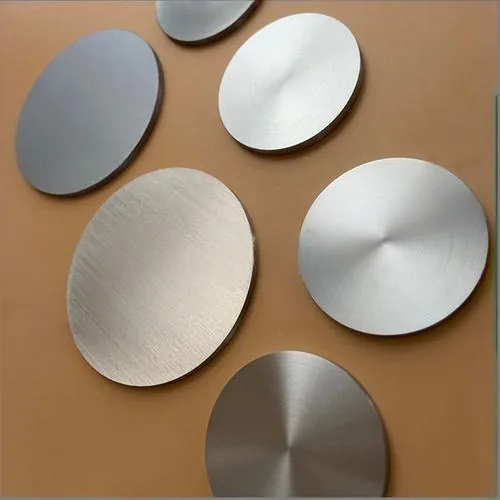
1. What is In₃SbTe₂ Sputtering Target?
The exponential growth of data-centric applications has placed unprecedented demands on memory technologies. Phase change memory (PCM) exploits the reversible transition between amorphous (high-resistance) and crystalline (low-resistance) phases in chalcogenide materials to store data.
The prototypical material Ge₂Sb₂Te₅ (GST) has been the subject of extensive research and commercial development due to its good cyclability, scalability, and reasonable switching speed [1]. However, as memory requirements push toward higher speeds and lower power consumption, the limitations of GST become increasingly apparent:
- Crystallization speed is constrained by nucleation-dominated kinetics
- Thermal stability is limited, with data retention degrading at elevated temperatures [2]
1.1 In₃SbTe₂ Sputtering Target
In₃SbTe₂ (IST) has emerged as a strong contender to address these shortcomings. Belonging to the In-Sb-Te ternary system, IST exhibits markedly different crystallization behavior and structural properties that endow it with remarkable speed and stability advantages over GST.
1.2 Article Overview
This article provides a comprehensive overview of IST as a sputtering target material and PCM active layer, examining:
- Fundamental properties
- Deposition methods
- Device characteristics
- Potential for next-generation high-speed storage applications
2. Fundamental Properties of In₃SbTe₂
2.1 Structural Characteristics
IST crystallizes in a structure distinct from the metastable rocksalt phase of GST. The phase transformation mechanism of IST involves a boundary reaction between InSb and InTe phases, which engenders a unique crystallization pathway compared to the nucleation-dominated process in GST [3].
This fundamental difference in crystallization mechanism leads to:
- Faster overall switching speeds
- More controlled phase transitions
The amorphous structure of IST is characterized by a higher degree of tetrahedral coordination compared to GST, contributing to its enhanced thermal stability. Pandey and Manivannan provided direct evidence for structural transformation in amorphous IST, showing that the material undergoes a unique structural rearrangement that stabilizes the amorphous phase against spontaneous crystallization [4].
Key Point: This structural characteristic is crucial for data retention performance.
2.2 Thermal Stability and Activation Energy
One of the most significant advantages of IST over GST is its superior thermal stability. Kim and Kim systematically compared the thermal properties of IST and GST using differential scanning calorimetry and thermal diffusivity measurements [2].
| Parameter | IST | GST |
|---|---|---|
| Activation energy for crystallization | 5.2 eV | 3.31 eV |
| Crystallization temperature | Higher (~250°C) | ~180°C |
This higher activation energy translates directly to:
- Improved amorphous-phase stability
- Longer data retention at elevated operating temperatures [2]
Jang et al. investigated the effect of In incorporation into SbTe matrices, revealing that In atoms strengthen the local bonding environment, raising the crystallization temperature and improving thermal stability [5].
Application: This makes IST particularly attractive for automotive and industrial applications where memory devices must withstand high-temperature environments.
2.3 Crystallization Kinetics
Understanding the crystallization kinetics is essential for predicting switching performance. Mu et al. employed ultrafast calorimetry to study the crystallization behavior of In-Sb-Te materials and demonstrated exceptionally fast crystallization kinetics rivaling the fastest known phase change materials [6].
| Material | Crystallization Mechanism | Characteristic |
|---|---|---|
| IST | Growth-dominated | Rapid, uniform transitions |
| GST | Nucleation-dominated | Slower, variable nucleation |
This growth-dominated crystallization contrasts with the nucleation-dominated mechanism in GST, enabling more rapid and uniform phase transitions at the nanoscale.
3. Sputtering Target Fabrication and Thin Film Deposition
3.1 Target Manufacturing
For large-scale PCM fabrication, sputtering remains the deposition method of choice due to its compatibility with existing semiconductor manufacturing processes.
IST sputtering target fabrication process:
- High-purity elemental precursors (99.999% In, 99.999% Sb, 99.999% Te)
- Stoichiometric mixing (In₃SbTe₂ composition)
- Hot-pressing or vacuum melting
- Quality verification
Target requirements:
- Uniform elemental distribution
- High density (>95% of theoretical density)
- Minimal contamination
Lee et al. demonstrated the successful fabrication of IST thin films using radio-frequency (RF) magnetron sputtering from a stoichiometric IST target [7]. Their results confirmed that sputtered IST films accurately reproduce the target composition and exhibit excellent uniformity over large substrate areas.
3.2 Film Deposition and Characterization
Typical sputtering parameters:
| Parameter | Range |
|---|---|
| Working gas | Ar |
| Pressure | 2–10 mTorr |
| RF power density | 1–5 W/cm² |
Process notes:
- As-deposited films are amorphous
- Post-deposition annealing or in-situ electrical pulsing used for crystallization
- Surface morphology is smooth and pinhole-free (critical for device reliability)
Saito et al. reviewed recent developments in sputter growth of chalcogenide-based phase-change materials, emphasizing that precise control over deposition parameters—including substrate temperature, sputtering power, and gas flow—is essential to achieve the desired stoichiometry and phase purity in ternary systems like IST [8].
Manufacturing milestone: The ability to deposit uniform IST films over 300 mm wafers has been demonstrated, confirming the manufacturability of this material.
4. Device Performance: In₃SbTe₂ vs. GST
4.1 Ultrafast Threshold Switching
Perhaps the most compelling advantage of IST is its ultrafast switching capability. Pandey and Manivannan investigated the threshold-switching dynamics of IST PCM devices at the picosecond timescale [9].
| Parameter | Value |
|---|---|
| Threshold voltage (Vᵢ) | 1.9 ± 0.1 V |
| Delay time at threshold | 25 ns |
| Delay time at 1.1 Vᵢ | 300 ± 50 ps |
Key finding: By increasing the applied voltage to just 1.1 Vᵢ, the delay time decreased exponentially to an astonishing value of 300 ± 50 ps—demonstrating sub-nanosecond switching that far exceeds the capabilities of conventional GST-based devices [9].
Saxena et al. further explored ultrafast threshold switching in IST devices, confirming that the material possesses intrinsic properties enabling electrical switching on the order of hundreds of picoseconds [10]. This speed is approaching the fundamental limit for phase change phenomena.
Additionally, Pandey et al. demonstrated that a weak electric field can assist the ultrafast electrical switching dynamics in IST, providing additional degrees of freedom for device engineering [11].
4.2 Multilevel Data Storage
IST exhibits exceptional multilevel storage capability, which is critical for increasing memory density without reducing cell dimensions.
Multilevel performance metrics:
| Metric | IST Performance |
|---|---|
| Optical states demonstrated | 8 states (3-bit) [13] |
| Thermal stability | Up to 260°C [13] |
| Reflectivity contrast | ≥1% between consecutive states |
| Noise variation | 0.18% (50% lower than GST) [13] |
| ON/OFF ratio | >3 orders of magnitude [14] |
Arjunan et al. demonstrated 8 uniform optical states (3-bit) by irradiating nanosecond laser pulses on thin IST films [13]. These states exhibited:
- High thermal stability up to 260°C
- At least 1% reflectivity contrast between consecutive states
- Noise variations measured at only 0.18% at each level—almost 50% lower than GST and AgInSbTe materials
Result: This ultralow noise enables a two-fold enhancement in signal-to-noise ratio, which is essential for reliable multilevel operation in photonic memory applications.
4.3 Chemical and Structural Phase Changes
The IST system exhibits a unique two-stage electrical phase change phenomenon. Lee et al. studied carbon-doped (1.5 wt.%) IST films and observed two distinct electrical phase changes [7]:
| Temperature | Phase Change Type | Description |
|---|---|---|
| 250°C | Chemical phase change | Formation of strong Sb–C bonds (no structural transition, remains amorphous) |
| 275°C | Structural phase change | Amorphous-to-crystalline transition |
This dual-phase-change behavior offers additional opportunities for engineering multilevel states.
Chen et al. observed chemical separation in IST thin films during phase transition, revealing that the crystallization process involves temporary phase segregation into InSb and InTe domains before forming the final crystalline structure [15].
4.4 Phase Transformation Mechanism
Kim et al. elucidated the phase transformation mechanism of IST as proceeding through a boundary reaction between InSb and InTe phases [3].
| GST | IST |
|---|---|
| “Umbrella flip” mechanism | Boundary reaction mechanism |
| Direct nucleation | In atom movement across domain boundaries |
| – | Rapid long-range ordering without extensive atomic diffusion |
This unique mechanism explains the exceptional switching speed of IST materials.
5. Comparative Analysis: IST vs. GST
5.1 Performance Comparison Table
| Property | In₃SbTe₂ (IST) | Ge₂Sb₂Te₅ (GST) |
|---|---|---|
| Activation energy of crystallization | 5.2 eV [2] | 3.31 eV [2] |
| Crystallization temperature | Higher (~250°C) [7] | ~180°C [7] |
| Threshold switching delay (at 1.1 Vᵢ) | ~300 ps [9] | ~ns range |
| Multilevel noise variation | 0.18% [13] | ~0.36% [13] |
| Crystallization mechanism | Growth-dominated [6] | Nucleation-dominated [1] |
| Data retention temperature | >260°C [13] | ~85-150°C |
5.2 Key Advantages of IST
- Higher activation energy (5.2 eV vs. 3.31 eV) → Superior data retention at elevated temperatures
- Sub-nanosecond switching at modest overvoltages (vs. nanoseconds for GST)
- Lower noise in multilevel operation (0.18% vs. 0.36%)
- Higher thermal stability for automotive/industrial applications
6. Applications and Future Outlook
The exceptional properties of IST position it as a leading candidate for several emerging application domains:
6.1 Storage-Class Memory (SCM)
IST’s combination of high speed and non-volatility makes it ideal for bridging the performance gap between DRAM and NAND Flash in SCM architectures.
6.2 Embedded PCM for Automotive
The high data retention temperature (>260°C) qualifies IST for automotive-grade memory applications that require reliable operation at elevated temperatures.
6.3 Photonic Memory
The low-noise multilevel switching and high reflectivity contrast in IST films make them excellent candidates for:
- Integrated photonic memory
- Neuromorphic computing platforms [13]
6.4 Neuromorphic Computing
The analog resistance tunability and multilevel switching characteristics of IST enable synaptic weight storage for artificial neural network accelerators.
6.5 Future Development
The development of high-quality IST sputtering targets and optimized deposition processes will be critical for commercialization. As semiconductor fabrication facilities adopt PCM into their manufacturing roadmaps, IST offers a drop-in compatible alternative to GST that delivers significant performance improvements.
7. Conclusion
In₃SbTe₂ represents a compelling alternative to conventional Ge₂Sb₂Te₅ for phase change memory applications, particularly where:
- High speed is required
- Thermal stability is critical
- Multilevel storage capability is needed
Key differentiators:
- Higher activation energy for crystallization (5.2 eV vs. 3.31 eV)
- Unique growth-dominated switching mechanism
- Sub-nanosecond threshold switching dynamics
- Low-noise multilevel states
- Excellent cycling endurance
- Compatibility with existing sputtering infrastructure
As the demand for faster, more reliable, and higher-density memory continues to grow, In₃SbTe₂ sputtering targets and devices are poised to play a transformative role in the evolution of storage technology. AtoZmat —— Advanced Materials from A to Z.
References
[1] S. K. Pandey and A. Manivannan, “Direct evidence for structural transformation and higher thermal stability of amorphous insbte phase change material,” Scripta Materialia, vol. 192, pp. 73–77, Feb. 2021. doi: 10.1016/j.scriptamat.2020.10.014
[2] Y. Tae Kim and S.-I. Kim, “Comparison of thermal stabilities between Ge-Sb-Te and In-Sb-Te phase change materials,” Applied Physics Letters, vol. 103, no. 12, Sep. 2013. doi: 10.1063/1.4821855
[3] Y. T. Kim, E. T. Kim, C. S. Kim, and J. Y. Lee, “Phase transformation mechanism of In–Sb–Te through the boundary reaction between InSb and InTe,” physica status solidi (RRL) – Rapid Research Letters, vol. 5, no. 3, pp. 98–100, Jan. 2011. doi: 10.1002/pssr.201004515
[4] S. K. Pandey and A. Manivannan, “Direct evidence for structural transformation and higher thermal stability of amorphous insbte phase change material,” Scripta Materialia, vol. 192, pp. 73–77, Feb. 2021. doi: 10.1016/j.scriptamat.2020.10.014
[5] M. H. Jang et al., “Effect of In incorporated into SbTe on phase change characteristics resulting from changes in electronic structure,” Applied Physics Letters, vol. 96, no. 5, Feb. 2010. doi: 10.1063/1.3308479
[6] S. Mu et al., “Understanding the fast crystallization kinetics of In–Sb–Te by using ultrafast calorimetry,” CrystEngComm, vol. 20, no. 2, pp. 159–163, 2018. doi: 10.1039/c7ce01787a
[7] Y. M. Lee, S. Y. Lee, T. Sasaki, K. Kim, D. Ahn, and M.-C. Jung, “Two different phase-change origins with chemical- and structural-phase-changes in C doped (1.5 wt.%) In3Sb1Te2,” Scientific Reports, vol. 6, Dec. 2016. doi: 10.1038/srep38663
[8] Y. Saito, M. Morota, K. Makino, J. Tominaga, A. V. Kolobov, and P. Fons, “Recent developments concerning the sputter growth of chalcogenide-based layered phase-change materials,” Materials Science in Semiconductor Processing, vol. 135, p. 106079, Nov. 2021. doi: 10.1016/j.mssp.2021.106079
[9] S. K. Pandey and A. Manivannan, “Sub-nanosecond threshold-switching dynamics and set process of In3SbTe2 phase-change memory devices,” Applied Physics Letters, vol. 108, no. 23, Jun. 2016. doi: 10.1063/1.4953196
[10] N. Saxena, C. Persch, M. Wuttig, and A. Manivannan, “Exploring ultrafast threshold switching in In3SbTe2 phase change memory devices,” Scientific Reports, vol. 9, no. 1, Dec. 2019. doi: 10.1038/s41598-019-55874-5
[11] S. K. Pandey, N. Saxena, and A. Manivannan, “A weak electric field-assisted ultrafast electrical switching dynamics in In3SbTe2 phase-change memory devices,” AIP Advances, vol. 7, no. 12, Dec. 2017. doi: 10.1063/1.4994184
[12] Y. I. Kim, E. T. Kim, J. Y. Lee, and Y. T. Kim, “Microstructures corresponding to multilevel resistances of In3Sb1Te2 phase-change memory,” Applied Physics Letters, vol. 98, no. 9, Mar. 2011. doi: 10.1063/1.3562024
[13] M. S. Arjunan, N. Saxena, A. Mondal, T. Dixit, K. N. V. D. Adarsh, and A. Manivannan, “High-Stability and Low-Noise Multilevel Switching in In3SbTe2 Material for Phase Change Photonic Memory Applications,” physica status solidi (RRL) – Rapid Research Letters, vol. 14, no. 12, 2020. doi: 10.1002/pssr.202000354
[14] N. Saxena, M. S. Arjunan, and A. Manivannan, “Extremely High Contrast Multi-Level Resistance States of In3SbTe2 Device for High Density Non-Volatile Memory Applications,” physica status solidi (RRL) – Rapid Research Letters, vol. 11, no. 11, 2017. doi: 10.1002/pssr.201700227
[15] Y. M. Chen, P. C. Kuo, W. T. Chao, and C. T. Kuo, “Observation of chemical separation of In3Sb1Te2 thin film during phase transition,” Applied Surface Science, vol. 293, pp. 363–367, Feb. 2014. doi: 10.1016/j.apsusc.2013.12.096