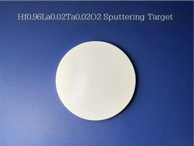
Hf0.96La0.02Ta0.02O2 represents a cutting-edge ceramic sputtering target material that enables the deposition of co-doped hafnium oxide thin films with exceptional ferroelectric properties for next-generation low-power memory and logic devices. This article comprehensively examines the material composition, fabrication methods, structural properties, and device applications of this advanced ceramic target. The dual doping strategy with lanthanum (La) and tantalum (Ta) synergistically stabilizes the ferroelectric orthorhombic phase in hafnium oxide while optimizing electrical performance parameters. We discuss the powder metallurgy approaches for target fabrication, sputtering deposition techniques, and the resulting thin film characteristics that make this material system particularly suitable for ferroelectric random-access memory (FeRAM), ferroelectric field-effect transistors (FeFETs), and neuromorphic computing applications requiring ultra-low power consumption.
What is Hf0.96La0.02Ta0.02O2?
The discovery of ferroelectricity in doped hafnium oxide (HfO_{2}) has revolutionized the field of non-volatile memory technology, offering a CMOS-compatible alternative to traditional perovskite ferroelectrics [1]. Unlike conventional ferroelectric materials such as Pb(Zr,Ti)O_{3} (PZT) or SrBi_{2}Ta_{2}O_{9} (SBT), which face significant integration challenges in modern semiconductor processes, hafnium oxide is already established as a high-k gate dielectric material in advanced CMOS technology nodes [2]. This inherent compatibility makes HfO_{2}-based ferroelectrics particularly attractive for scaling to sub-10 nm technology nodes.
The ferroelectric properties in HfO_{2} are induced through doping with various elements that stabilize the non-centrosymmetric orthorhombic phase (space group Pca2_{1}) [3]. Among the numerous dopants investigated, lanthanum has emerged as one of the most effective for achieving high remanent polarization values and robust ferroelectric behavior [4]. The addition of tantalum as a co-dopant further enhances the material’s electrical properties and thermal stability, making the Hf0.96La0.02Ta0.02O2 composition particularly promising for practical device applications.
Material Composition and Phase Stabilization
Dual Doping Strategy
The Hf0.96La0.02Ta0.02O2 composition employs a sophisticated dual doping approach where lanthanum (La^{3+}) and tantalum (Ta^{5+}) ions substitute for hafnium (Hf^{4+}) sites in the oxide lattice. The ionic radius mismatch between these dopants and the host Hf^{4+} ions (La^{3+}: 1.16 Å, Ta^{5+}: 0.64 Å, Hf^{4+}: 0.71 Å) creates lattice strain that promotes the stabilization of the ferroelectric orthorhombic phase over the thermodynamically stable monoclinic phase [5].
Lanthanum doping at 2% concentration has been shown to provide optimal ferroelectric properties, with remanent polarization values exceeding 30 μC/cm^{2} in optimized films [6]. The larger La^{3+} ions introduce tensile strain in the lattice, while the smaller Ta^{5+} ions (at 2% concentration) introduce compressive strain, creating a balanced stress state that enhances phase stability and reduces leakage currents [7].
Phase Diagram and Structural Properties
The phase stability of doped HfO_{2} is highly dependent on dopant concentration, film thickness, and thermal processing conditions. Studies have shown that La-doped HfO_{2} exhibits a broad processing window for ferroelectric phase formation, making it more manufacturable than other dopant systems [8]. The addition of Ta further widens this processing window and improves the thermal stability of the ferroelectric phase during subsequent device fabrication steps.
X-ray diffraction analysis of films deposited from Hf0.96La0.02Ta0.02O2 targets typically reveals a mixture of orthorhombic and tetragonal phases, with the orthorhombic phase fraction increasing with proper annealing treatments [9]. The coexistence of these phases can be beneficial for certain device applications, as the tetragonal phase contributes to higher dielectric constant while the orthorhombic phase provides the ferroelectric switching behavior.
Sputtering Target Fabrication
Powder Synthesis and Processing
The fabrication of Hf0.96La0.02Ta0.02O2 sputtering targets begins with the synthesis of high-purity precursor powders. Typically, hafnium oxide (HfO_{2}), lanthanum oxide (La_{2}O_{3}), and tantalum oxide (Ta_{2}O_{5}) powders with purity levels exceeding 99.99% are used as starting materials. These powders are carefully weighed according to the stoichiometric ratio and subjected to intensive mixing processes to ensure homogeneous distribution of dopants [10].
Several mixing techniques can be employed, including:
- Ball milling: Using zirconia or alumina balls in alcohol or water-based media
- Attrition milling: For finer particle size distribution and better homogeneity
- High-energy planetary milling: To achieve nanoscale mixing and reduce subsequent sintering temperatures
Consolidation and Sintering
After thorough mixing, the powder blend undergoes consolidation through various pressing techniques:
- Uniaxial pressing: Simple and cost-effective but may result in density gradients
- Cold isostatic pressing (CIP): Provides more uniform density distribution throughout the target
- Spark plasma sintering (SPS): Enables rapid consolidation at lower temperatures, minimizing grain growth and maintaining fine microstructure
The sintering process is critical for achieving the required density (typically >95% of theoretical density) and mechanical strength. Conventional sintering is performed in controlled atmosphere furnaces at temperatures ranging from 1400°C to 1600°C, depending on the specific powder characteristics and sintering aids used [11].
Advanced sintering techniques such as hot pressing (HP) and hot isostatic pressing (HIP) can further improve density and eliminate residual porosity, which is essential for preventing arcing during sputtering and ensuring uniform film deposition.
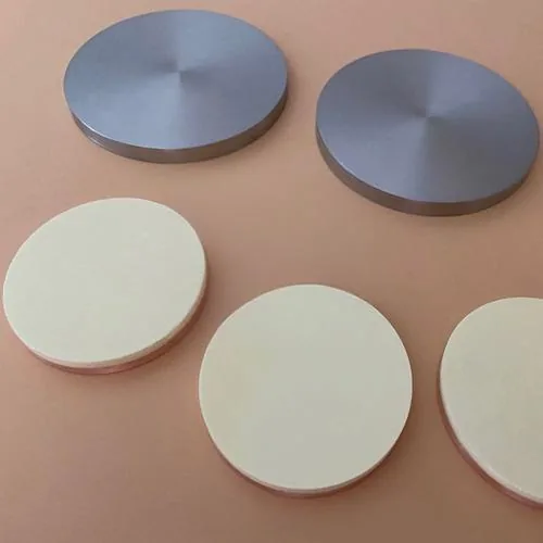
Target Bonding and Finishing
Once sintered, the ceramic target must be bonded to a metallic backing plate (typically copper or aluminum) to facilitate efficient heat dissipation during sputtering. Various bonding methods are employed:
- Indium bonding: Provides excellent thermal conductivity but limited to lower temperature applications
- Epoxy bonding: Simple but may outgas during sputtering
- Metallic bonding (soldering or brazing): Offers good thermal and electrical conductivity
- Diffusion bonding: Creates a metallurgical bond without intermediate layers, ideal for high-power applications
The bonded target assembly undergoes final machining to achieve precise dimensional tolerances and surface finish requirements. The target surface is typically ground and polished to a mirror finish (Ra < 0.4 μm) to ensure uniform erosion during sputtering and minimize particle generation [12].
Sputtering Deposition and Film Properties
Deposition Parameters
Thin films deposited from Hf0.96La0.02Ta0.02O2 targets using magnetron sputtering exhibit excellent properties when optimized deposition conditions are employed:
- Sputtering pressure: 1-10 mTorr in Ar or Ar/O_{2} mixtures
- Power density: 1-5 W/cm^{2} for RF sputtering
- Substrate temperature: Room temperature to 400°C
- Post-deposition annealing: 400-700°C in N_{2} or forming gas atmosphere
Reactive sputtering from metallic Hf-La-Ta targets can also be employed, but ceramic target sputtering offers better process stability and composition control, especially for complex multi-component oxides [13].
Structural and Electrical Characteristics
Films deposited from Hf0.96La0.02Ta0.02O2 targets typically exhibit:
- Thickness uniformity: Better than ±5% across 200 mm wafers
- Compositional uniformity: Dopant distribution within ±0.2 at.% of target composition
- Crystallographic properties: Predominantly orthorhombic phase with grain sizes of 10-30 nm
Electrical properties:
- Remanent polarization (Pr): 25-35 μC/cm^{2}
- Coercive field (Ec): 1-2 MV/cm
- Dielectric constant (k): 25-35
- Leakage current density: <10^{-7} A/cm^{2} at 2 MV/cm
The dual doping approach provides several advantages over single-doped systems:
- Enhanced polarization stability: Reduced wake-up effect and imprint
- Improved endurance: >10^{10} switching cycles demonstrated
- Lower leakage currents: Due to reduced oxygen vacancy concentration
- Better thermal stability: Maintains ferroelectric properties up to 500°C
Device Applications
Ferroelectric Random-Access Memory (FeRAM)
Hf0.96La0.02Ta0.02O2-based FeRAM devices offer significant advantages over conventional perovskite-based FeRAM:
- CMOS compatibility: Direct integration with existing fabrication processes
- Scalability: Demonstrated functionality at sub-20 nm dimensions
- Low power operation: Field-driven switching with minimal current flow
- Fast switching: Sub-nanosecond polarization reversal possible
The 1T-1C (one transistor, one capacitor) cell structure benefits from the high Pr values and low Ec of La/Ta co-doped HfO_{2}, enabling smaller capacitor areas and higher density memory arrays [14].
Ferroelectric Field-Effect Transistors (FeFETs)
FeFETs utilizing Hf0.96La0.02Ta0.02O2 as the gate dielectric enable novel memory and logic functions:
- Non-volatile memory: Data retention exceeding 10 years at 85°C
- Logic-in-memory: Enables new computing architectures
- Low-voltage operation: <3 V programming voltages
- Multi-level cell capability: Multiple distinct polarization states for higher storage density
The compatibility with high-k metal gate (HKMG) technology allows seamless integration into advanced CMOS nodes, making FeFETs particularly attractive for embedded non-volatile memory applications [15].
Neuromorphic Computing
The analog switching characteristics and multi-state capability of Hf0.96La0.02Ta0.02O2-based devices make them ideal for neuromorphic computing applications:
- Synaptic weight storage: Continuous polarization modulation mimics biological synapses
- Energy efficiency: Field-driven switching minimizes power consumption
- Scalability: Enables high-density crossbar arrays for neural network implementation
- Linearity and symmetry: Improved device-to-device uniformity for accurate weight updates
Recent demonstrations have shown that HfO_{2}-based ferroelectric memcapacitors can achieve energy efficiencies exceeding traditional von Neumann architectures by several orders of magnitude for certain computational tasks [16].
Challenges and Future Perspectives
Technical Challenges
Despite the promising properties of Hf0.96La0.02Ta0.02O2, several challenges remain:
- Interface engineering: Optimizing electrode interfaces to minimize dead layers and interface traps
- Scalability limits: Understanding fundamental limits of ferroelectricity in ultra-thin films (<5 nm)
- Reliability: Improving endurance and retention at elevated temperatures
- Variability: Reducing device-to-device and cycle-to-cycle variations
Manufacturing Considerations
For commercial adoption, several manufacturing aspects need attention:
- Target cost reduction: Developing more economical powder synthesis and sintering methods
- Process integration: Establishing design rules and process modules for foundry implementation
- Metrology: Developing accurate characterization techniques for ferroelectric thin films
- Standardization: Creating industry standards for material specifications and device testing
Future Research Directions
Future research on Hf0.96La0.02Ta0.02O2 and related materials should focus on:
- Advanced doping strategies: Exploring ternary and quaternary doping for further property optimization
- Interface control: Atomic layer engineering of electrode/ferroelectric interfaces
- 3D integration: Developing processes for vertical FeRAM and FeFET structures
- Beyond memory applications: Exploring piezoelectric, pyroelectric, and electrocaloric applications
- Machine learning optimization: Using computational methods to discover optimal doping combinations and processing conditions
Conclusion
Hf0.96La0.02Ta0.02O2 sputtering targets represent a significant advancement in materials for low-power memory and logic devices. The dual doping strategy with lanthanum and tantalum provides an optimal balance of ferroelectric properties, thermal stability, and process compatibility. The ceramic target fabrication methods have matured to produce high-quality, dense targets suitable for industrial-scale sputtering deposition.
The resulting thin films exhibit excellent ferroelectric characteristics that enable a new generation of memory devices with superior performance compared to existing technologies. As research continues to address the remaining challenges and optimize device integration, Hf0.96La0.02Ta0.02O2-based technologies are poised to play a crucial role in enabling energy-efficient computing systems for artificial intelligence, Internet of Things, and other emerging applications that demand ultra-low power non-volatile memory solutions.
The combination of CMOS compatibility, excellent electrical properties, and scalability makes this material system particularly promising for widespread adoption in both standalone and embedded memory applications, potentially revolutionizing the memory hierarchy in future computing systems.
AtoZmat —— Advanced Materials from A to Z.
References
[1] Schroeder, U.; Richter, C.; Park, M. H.; Schenk, T.; Pešić, M.; Hoffmann, M.; Fengler, F. P. G.; Pohl, D.; Rellinghaus, B.; Zhou, C.; Chung, C.-C.; Jones, J. L.; Mikolajick, T. Lanthanum-Doped Hafnium Oxide: A Robust Ferroelectric Material. Inorganic Chemistry 2018, 57 (5), 2752–2765. DOI: 10.1021/acs.inorgchem.7b03149
[2] Mikolajick, T.; Slesazeck, S.; Park, M. H.; Schroeder, U. Ferroelectric Hafnium Oxide for Ferroelectric Random-Access Memories and Ferroelectric Field-Effect Transistors. MRS Bulletin 2018, 43 (5), 340–346. DOI: 10.1557/mrs.2018.92
[3] Starschich, S.; Boettger, U. An Extensive Study of the Influence of Dopants on the Ferroelectric Properties of HfO_{2}. Journal of Materials Chemistry C 2017, 5 (2), 333–338. DOI: 10.1039/c6tc04807b
[4] Mikolajick, T.; Schroeder, U.; Lomenzo, P. D.; Breyer, E. T.; Mulaosmanovic, H.; Hoffmann, M.; Mittmann, T.; Mehmood, F.; Max, B.; Slesazeck, S. Next Generation Ferroelectric Memories Enabled by Hafnium Oxide. In 2019 IEEE International Electron Devices Meeting (IEDM); IEEE, 2019; p 15.5.1-15.5.4. DOI: 10.1109/iedm19573.2019.8993447
[5] Wang, X.; Ye, S.; Cui, B.; Li, Y.-C.; Wei, Y.; Xiao, Y.; Liu, J.; Huang, Z.-Y.; Wu, Y.; Wen, Y.; Wang, Z.; Wu, M.; Ren, P.; Fang, H.; Lu, H.-L.; Wang, R.; Ji, Z.; Huang, R. Hafnium Oxide-Based Nonvolatile Ferroelectric Memcapacitor Array for High Energy-Efficiency Neuromorphic Computing. Nano Energy 2025, 140, 111011. DOI: 10.1016/j.nanoen.2025.111011
[6] Sharma, U.; Singh, C.; Varma, V. M.; Kumar, G.; Mishra, S.; Kumar, A.; Thomas, R. Preparation and Characterization of Hafnium-Zirconium Oxide Ceramics as a CMOS Compatible Material for Non-Volatile Memories. Bulletin of Materials Science 2023, 46 (2). DOI: 10.1007/s12034-022-02887-y
[7] Ceramic Target Materials for Sputtering Applications. Materials Science Forum 2010, 638-642, 805–810. DOI: 10.4028/www.scientific.net/msf.638-642.805
[8] Impact of Varying Wet Oxidation Temperature in the Presence of Nitrogen Flow on Hafnium Tantalum Oxide Films. Ceramics International 2023, 49 (23), 38765–38773. DOI: 10.1016/j.ceramint.2023.09.076
[9] Endurance of Ferroelectric La-doped HfO_{2} for SFS Gate-Stack Memory Devices. In 2020 IEEE International Memory Workshop (IMW); IEEE, 2020; p 1–4. DOI: 10.1109/imw48823.2020.9108125
[10] Properties of Dopants in HfO_{x} for Improving the Performance of Nonvolatile Memory. Physical Review Applied 2017, 7 (3), 034020. DOI: 10.1103/physrevapplied.7.034020
[11] Fabrication and Characterisation of Memristor Device Using Sputtered Hafnium Oxide. Journal of Materials Science: Materials in Electronics 2023, 34 (5). DOI: 10.1007/s10854-023-10613-5
[12] Electrical Characteristics Investigation of Ferroelectric Memories Using Stacked and Mixed Hafnium Zirconium Oxides. Thin Solid Films 2022, 742, 139395. DOI: 10.1016/j.tsf.2022.139395