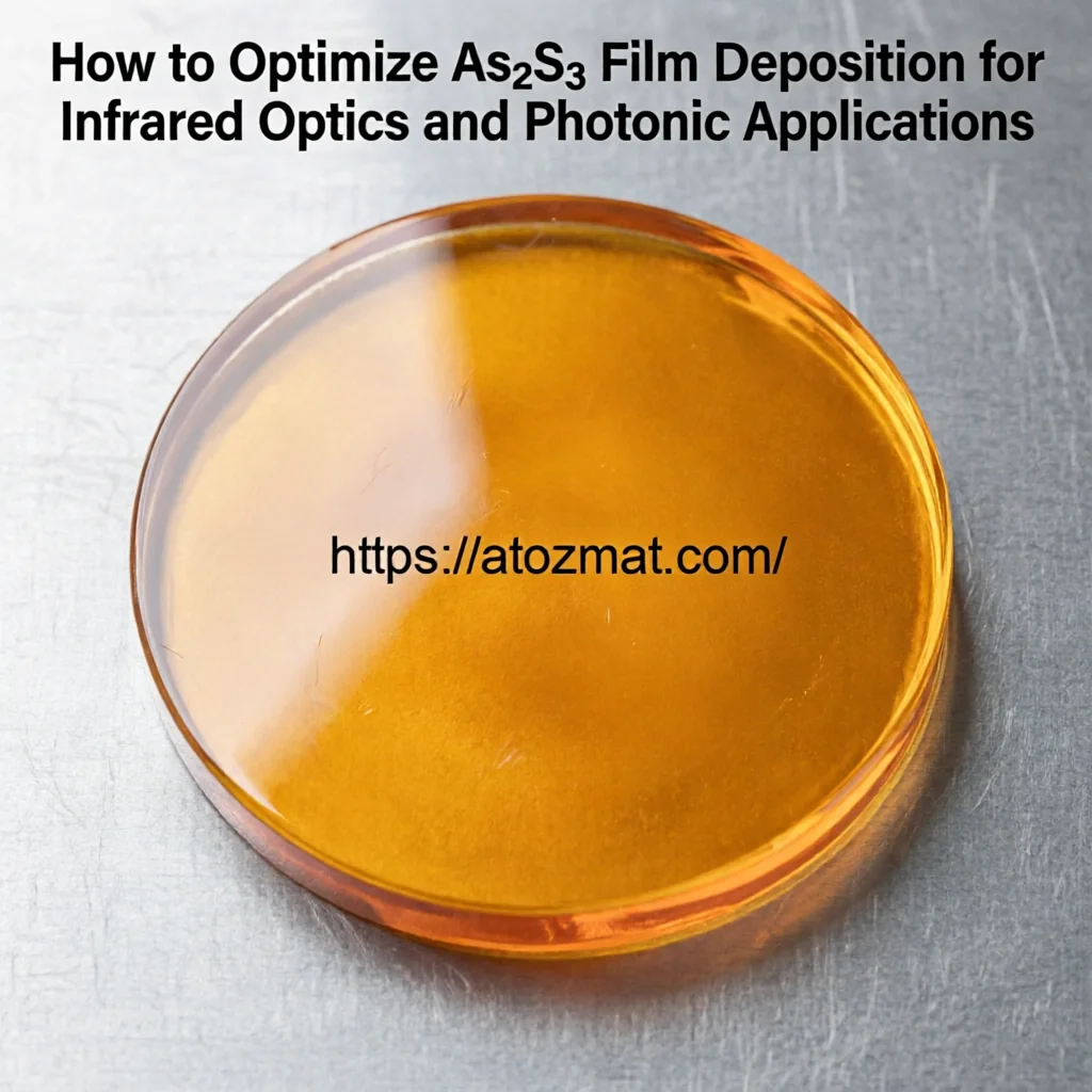
Why Arsenic Sulfide Matters in Thin Film Applications
Arsenic sulfide belongs to the chalcogenide glass family and offers exceptional infrared transparency, making it valuable for mid-infrared optical coatings, waveguides, and sensing applications. The material transmits well in the 2–12 μm wavelength range, which is critical for thermal imaging, spectroscopy, and chemical sensing systems. Recent research has focused on As₂S₃ films for integrated photonics, where low optical loss and high refractive index contrast enable compact waveguide designs.
Beyond optics, As₂S₃ films show promise in phase-change memory devices and resistive switching applications. Researchers have demonstrated reversible structural transitions between amorphous and crystalline states, with switching speeds in the nanosecond range under controlled electrical pulses. These properties position arsenic sulfide as a candidate material for next-generation non-volatile memory architectures.
Material Properties and Film Characteristics
Sputtered As₂S₃ films typically exhibit amorphous structure as-deposited, with refractive indices ranging from 2.3 to 2.5 at 1550 nm depending on deposition conditions and film density. The optical bandgap generally falls between 2.2 and 2.4 eV, though this can shift with compositional variations or thermal treatment.
Key material properties include:
- Infrared transparency: High transmission from 2 μm to beyond 10 μm, with absorption edges determined by film quality and stoichiometry
- Refractive index: Tunable through deposition parameters, typically 2.3–2.5 in the near-infrared
- Thermal stability: Glass transition temperature around 180–200°C for stoichiometric films
- Density: Sputtered films typically achieve 85–95% of bulk density depending on process conditions
- Surface roughness: Well-optimized processes yield RMS roughness below 1 nm for optical-quality films
Film stoichiometry represents a critical control parameter. Arsenic-rich or sulfur-deficient films can exhibit different optical properties and crystallization behavior compared to stoichiometric As₂S₃. Researchers commonly use X-ray photoelectron spectroscopy (XPS) or energy-dispersive X-ray spectroscopy (EDS) to verify composition, targeting As:S ratios close to 2:3.
Deposition Parameters and Process Optimization
RF magnetron sputtering is the most common deposition method for As₂S₃ films, offering better stoichiometry control than DC sputtering for compound targets. Typical process parameters reported in the research literature include:
- RF power density: 1–3 W/cm² for stable plasma conditions without target overheating
- Working pressure: 3–10 mTorr argon, with lower pressures generally producing denser films
- Substrate temperature: Room temperature to 150°C; higher temperatures can improve film density but risk compositional changes
- Deposition rate: 5–20 nm/min depending on power and geometry
- Target-substrate distance: 5–10 cm for uniform coverage in research systems
Substrate temperature significantly affects film properties. Room-temperature deposition produces fully amorphous films with lower density, while moderate heating (80–120°C) can improve film packing without inducing crystallization. Temperatures above 180°C risk approaching the glass transition point, potentially causing compositional drift or surface roughening.
Base pressure before deposition should reach at least 1×10⁻⁶ Torr to minimize oxygen and water vapor incorporation. Even small amounts of oxygen contamination can increase optical absorption in the infrared and degrade film stability. Some research groups use argon pre-sputtering to clean the target surface before film deposition begins.
Applications in Infrared Optics and Photonics
As₂S₃ films serve multiple roles in infrared optical systems:
Anti-reflection coatings: The high refractive index and broad infrared transparency make As₂S₃ suitable for single-layer or multilayer AR coatings on germanium, silicon, or chalcogenide optics. Engineers typically design coating stacks for 3–5 μm or 8–12 μm atmospheric windows.
Planar waveguides: Integrated photonic circuits for mid-infrared sensing and spectroscopy use As₂S₃ as the core layer, with lower-index cladding materials providing optical confinement. Researchers have demonstrated waveguide propagation losses below 1 dB/cm at 3.5 μm in optimized films.
Photonic crystals and gratings: The material’s etch compatibility and high index contrast enable fabrication of periodic structures for wavelength filtering and beam steering in the mid-infrared.
Nonlinear optics: As₂S₃ exhibits strong third-order nonlinearity, making it attractive for supercontinuum generation and four-wave mixing experiments in the infrared. Film quality and uniformity directly impact nonlinear device performance.
Emerging Research Directions
Current research explores several advanced applications for As₂S₃ thin films:
Phase-change memory: Electrical switching between amorphous and crystalline states offers potential for non-volatile memory devices. Researchers investigate doping strategies and interface engineering to improve switching speed, cyclability, and retention characteristics.
Photonic integration: Combining As₂S₃ waveguides with silicon photonics platforms enables hybrid devices that extend functionality into the mid-infrared. Challenges include thermal expansion mismatch and adhesion optimization.
Flexible optics: Deposition on polymer substrates for flexible infrared optics and sensors requires careful control of substrate temperature and film stress to prevent cracking or delamination.
Compositional tuning: Adjusting the As:S ratio or adding elements like selenium or germanium allows researchers to tailor optical properties, glass transition temperature, and crystallization behavior for specific applications.
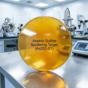
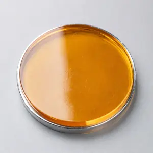
Target Selection and Procurement Considerations
When sourcing As₂S₃ sputtering targets, engineers should evaluate several factors:
Purity: High-purity targets (99.99% or better) minimize contamination that could increase optical absorption or affect film stoichiometry. Trace metal impurities are particularly problematic for optical applications.
Density: Targets should be fabricated to high density (typically >95% of theoretical) to ensure consistent sputtering behavior and reduce particulate generation. Hot-pressed or sintered targets generally perform better than cast materials.
Bonding: Arsenic sulfide is brittle and requires careful bonding to backing plates. Indium or elastomer bonding methods accommodate thermal expansion differences and reduce cracking risk during use.
Size and geometry: Common research-scale targets include 2-inch and 3-inch diameters with 1/8-inch or 1/4-inch thickness. Larger targets for production systems require careful quality control to maintain uniformity.
Handling precautions: Arsenic compounds require appropriate safety protocols. Targets should be stored in inert atmosphere or vacuum packaging to prevent oxidation or moisture absorption.
Common Deposition Challenges
Process engineers frequently encounter specific issues when working with As₂S₃ targets:
Stoichiometry drift: Preferential sputtering can cause composition changes over extended runs. Monitoring film properties and adjusting power or pressure helps maintain consistency.
Target cracking: Thermal stress during sputtering can crack brittle chalcogenide targets. Gradual power ramp-up and proper cooling reduce this risk.
Film stress: As-deposited films often exhibit tensile stress that can cause cracking in thick layers. Substrate heating or post-deposition annealing may help, though temperature must stay below the glass transition point.
Adhesion: As₂S₃ films may require adhesion layers on some substrates. Thin chromium or titanium interlayers (5–10 nm) can improve adhesion without significantly affecting optical properties.
Oxidation sensitivity: Exposure to atmosphere can degrade film surfaces over time. Protective capping layers or immediate device integration help preserve film quality.
Quality Assessment Methods
Characterizing As₂S₃ films requires multiple analytical techniques:
- Spectroscopic ellipsometry: Determines refractive index, extinction coefficient, and film thickness with high precision
- FTIR spectroscopy: Verifies infrared transmission and identifies absorption features from impurities or compositional variations
- XRD: Confirms amorphous structure and detects any crystalline phases
- XPS or EDS: Measures elemental composition and stoichiometry
- AFM or profilometry: Assesses surface roughness and film uniformity
- Stress measurement: Wafer curvature methods quantify film stress for thick coating applications
Practical Selection Guide
Engineers selecting As₂S₃ sputtering targets should consider their specific application requirements:
For infrared optical coatings, prioritize high-purity targets and optimize deposition for low surface roughness and minimal absorption. Film thickness uniformity across the substrate becomes critical for multi-element optics.
For photonic waveguide applications, focus on achieving consistent refractive index and low propagation loss. This typically requires careful control of deposition rate, substrate temperature, and base pressure.
For phase-change memory research, compositional control and the ability to achieve both amorphous and crystalline phases through thermal or electrical treatment take priority. Film adhesion and interface quality with electrode materials also matter.
For research and development work, smaller targets (2–3 inch diameter) offer cost-effective material exploration. Production environments benefit from larger targets that provide longer run times and better batch-to-batch consistency.
Conclusion
Optimizing As₂S₃ film deposition requires balancing multiple process parameters to achieve the desired optical, structural, and compositional properties. Understanding the relationships between sputtering conditions, film characteristics, and application requirements enables engineers to develop robust processes for infrared optics, photonic devices, and emerging memory technologies. Careful target selection, process control, and characterization methods ensure consistent film quality for both research and production environments.
Product Information
For technical specifications and availability of arsenic sulfide sputtering targets, visit: Arsenic Sulfide Sputtering Targets (As₂S₃) | atozmat