Aluminum-doped zinc oxide (AZO) sputtering targets have become essential tools in thin film deposition for transparent conductive oxide (TCO) applications. Engineers working on optoelectronic devices, solar cells, flat panel displays, and touch screen technologies rely on AZO targets to deposit films that combine optical transparency with electrical conductivity—a combination critical for modern electronic and photovoltaic systems.
The performance of AZO thin films depends heavily on target quality, deposition parameters, and process control. Understanding how to optimize these factors helps engineers achieve consistent film properties and avoid common deposition challenges.
AZO targets consist of zinc oxide doped with aluminum oxide, typically in the range of 1-5 wt% Al₂O₃. The aluminum acts as an n-type dopant, introducing free electrons into the ZnO lattice and dramatically improving electrical conductivity while maintaining high optical transmission in the visible spectrum.
Unlike pure zinc oxide, which exhibits relatively poor electrical properties, AZO films can achieve resistivities as low as 2-4 × 10⁻⁴ Ω·cm while maintaining optical transmission above 85% in the visible range. This combination makes AZO competitive with indium tin oxide (ITO) in many applications, with the added benefits of lower material cost and better thermal stability.
Target density and microstructure significantly affect film quality. High-density targets (typically >95% theoretical density) produce more uniform films with fewer particulates. Grain structure also matters—targets with controlled grain size and orientation can improve sputtering uniformity and reduce arcing during deposition.
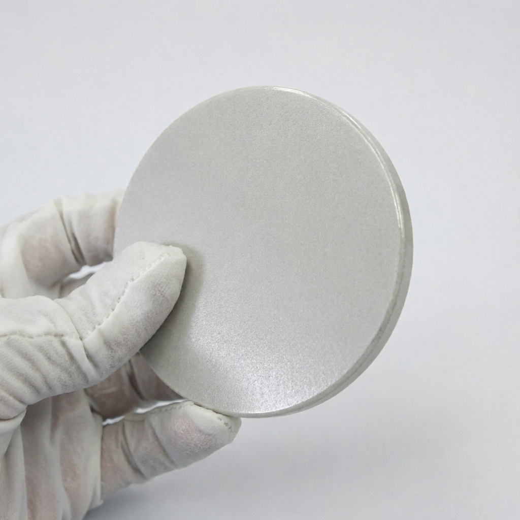
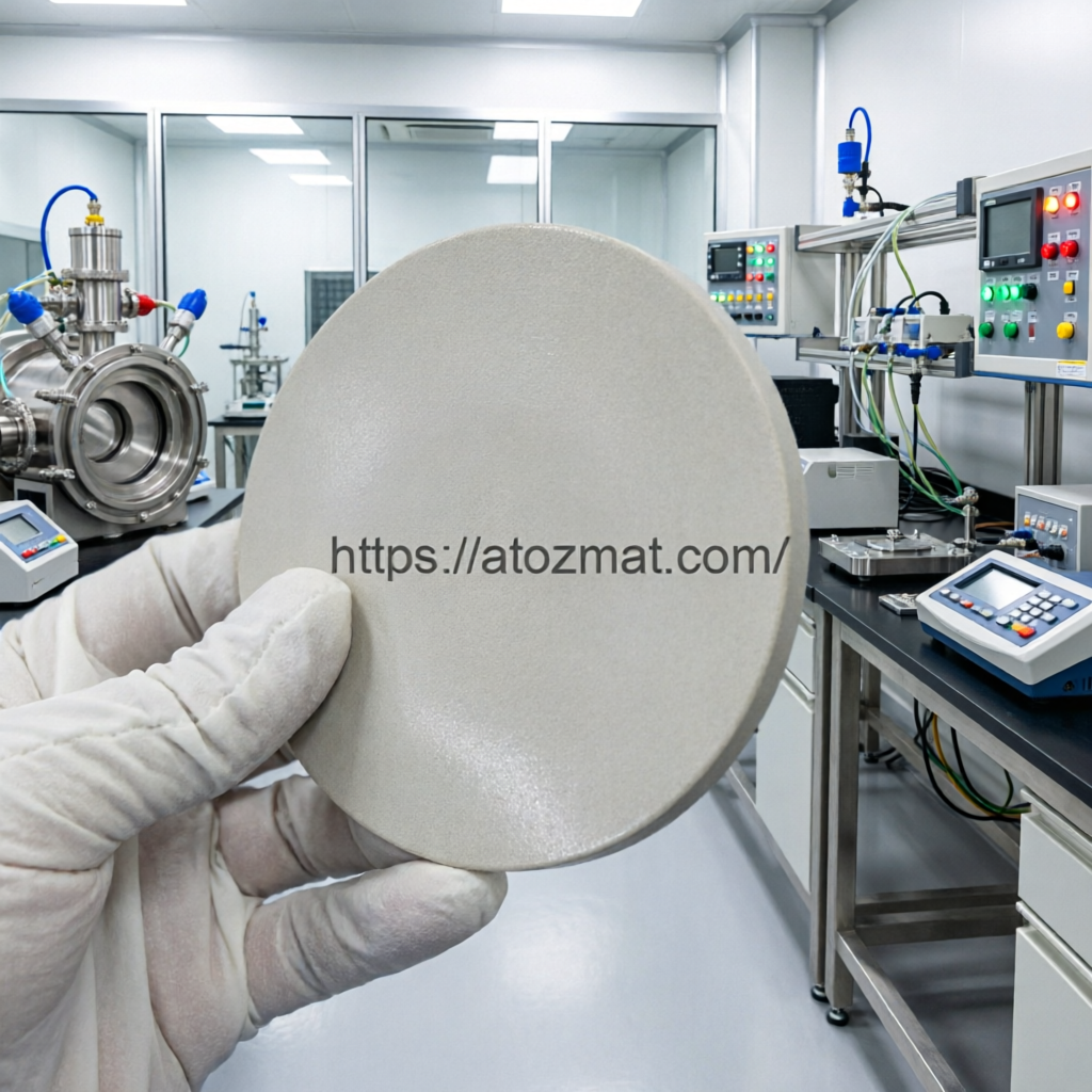
Research laboratory application context for Aluminum Doped Zinc Oxide Sputtering Targets (Al2O3-ZnO Sputtering Targets) | AZO-ST
Key Deposition Parameters for Film Optimization
Achieving high-quality AZO films requires careful control of several process variables. Substrate temperature plays a critical role in film crystallinity and electrical properties. Research shows that deposition temperatures between 200-400°C typically produce films with optimal conductivity and transparency. Lower temperatures may result in amorphous or poorly crystallized films with higher resistivity, while excessive temperatures can lead to aluminum segregation or unwanted phase formation.
Sputtering power and pressure also significantly impact film properties. DC or RF magnetron sputtering at powers ranging from 50-300 W (depending on target size) with argon pressures between 1-10 mTorr represents common operating ranges. Higher power generally increases deposition rate but may introduce more defects if not properly controlled. Typical deposition rates for AZO range from 5-50 nm/min depending on power, pressure, and target-to-substrate distance.
Oxygen partial pressure during deposition requires particularly careful attention. While AZO targets already contain oxygen in the ZnO matrix, introducing controlled oxygen flow (typically 0-5% O₂ in argon) can help compensate for oxygen deficiency in the growing film. However, excessive oxygen can reduce conductivity by filling oxygen vacancies that contribute to n-type doping. Engineers often optimize this parameter through systematic testing to balance optical and electrical properties.
Applications Driving AZO Target Demand
Thin film photovoltaics represent one of the largest application areas for AZO films. In CIGS (copper indium gallium selenide) and CdTe solar cells, AZO serves as a transparent front contact that allows light to reach the absorber layer while collecting photogenerated carriers. The material’s high transparency in the solar spectrum and good electrical conductivity make it well-suited for this role. Recent research focuses on improving AZO film uniformity over large areas and optimizing its interface with adjacent layers to minimize optical and electrical losses.
Flat panel display manufacturing uses AZO as a transparent electrode material, particularly in applications where ITO’s brittleness or cost presents challenges. Touch screen panels, LCD displays, and emerging flexible display technologies all benefit from AZO’s combination of conductivity, transparency, and mechanical properties. The material’s better resistance to hydrogen plasma (compared to ITO) also makes it attractive for certain display manufacturing processes.
Optoelectronic devices including LEDs, photodetectors, and thin film transistors increasingly incorporate AZO layers. The material serves as transparent contacts, current spreading layers, or active channel materials depending on the device architecture. Research in this area explores optimizing AZO film properties for specific device requirements, such as work function tuning for improved carrier injection or mobility enhancement for transistor applications.
Selection Factors for Engineers and Buyers
Target composition represents the first critical selection factor. While 2 wt% Al₂O₃ doping is common, some applications benefit from higher or lower doping levels. Higher aluminum content generally increases conductivity but may reduce optical transmission and film stability. Engineers should consider their specific application requirements when selecting doping concentration.
Target purity affects film contamination and device performance. High-purity targets (99.9% or better) minimize unwanted impurities that can degrade electrical properties or introduce optical absorption. For research applications or high-performance devices, 99.99% or higher purity may be necessary. However, higher purity typically increases cost, so engineers must balance purity requirements against budget constraints.
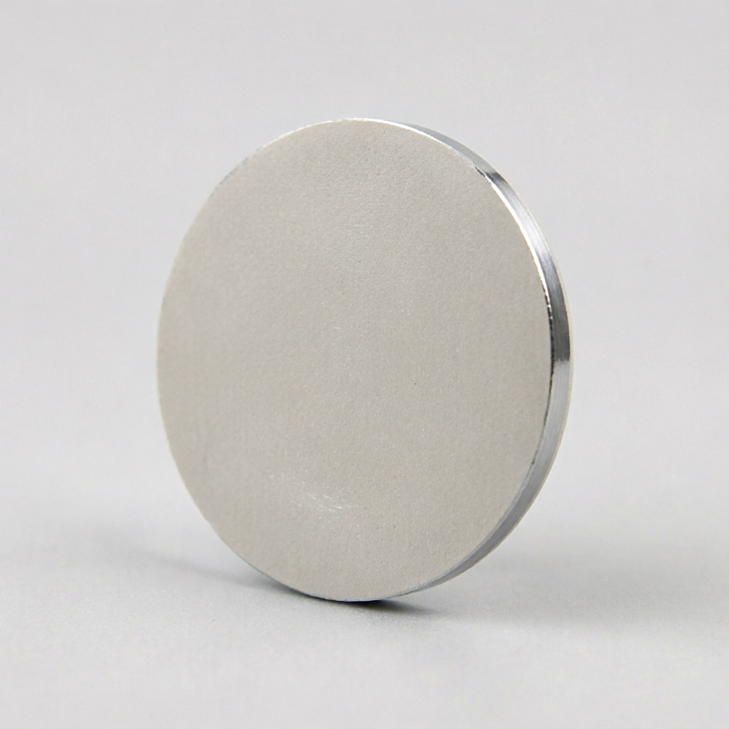
Physical dimensions and bonding configuration must match the deposition system. Common circular target sizes include 2-inch, 3-inch, and 4-inch diameters with thicknesses ranging from 1/8 inch to 1/4 inch. Larger targets are available for production systems. Backing plate material and bonding method (indium bonding, elastomer bonding, or direct bonding) should be specified based on system requirements and thermal management needs.
Target density and microstructure quality impact both film uniformity and target lifetime. Dense, well-sintered targets with uniform grain structure provide more consistent sputtering behavior and longer service life. Engineers should inquire about manufacturing methods and quality control procedures when evaluating suppliers.
Common Challenges and Solutions
Film uniformity across large substrates presents a persistent challenge in AZO deposition. Non-uniform thickness or composition can result from target erosion patterns, magnetic field configuration, or substrate positioning. Using rotating substrate holders, optimizing target-to-substrate distance (typically 5-15 cm), and implementing target rotation or rastering can improve uniformity. Some engineers also use pre-sputtering to establish stable target surface conditions before depositing on production substrates.
Particle generation during sputtering can degrade film quality and device yield. Particles may originate from target cracking, flaking, or arcing. Using high-density targets, proper target conditioning, and appropriate power ramping procedures helps minimize particle issues. Regular system maintenance and target inspection also play important roles in particle control.
Film stability and aging behavior require consideration for long-term device reliability. AZO films can exhibit resistivity increases over time due to oxygen adsorption or structural relaxation. Post-deposition annealing in controlled atmospheres, protective capping layers, or composition optimization can improve film stability. Recent research explores dopant combinations and deposition conditions that produce more stable films.
Current Research Directions
The research community continues to explore ways to improve AZO film properties and expand application possibilities. Work on co-doping strategies—adding small amounts of additional elements like gallium, indium, or fluorine—aims to further enhance conductivity or stability. These approaches show promise for achieving ITO-comparable performance at lower cost.
Flexible electronics applications drive research into low-temperature AZO deposition methods. Achieving good film properties at substrate temperatures below 150°C would enable deposition on plastic substrates for flexible displays, wearable electronics, and roll-to-roll manufacturing. Techniques including pulsed laser deposition, atomic layer deposition, and optimized sputtering conditions are being investigated for this purpose.
Interface engineering between AZO and adjacent layers receives increasing attention as device structures become more complex. Understanding and controlling band alignment, work function, and chemical interactions at AZO interfaces can improve device efficiency and reliability. This work has implications for solar cells, LEDs, and thin film transistors.
Practical Considerations for Implementation
Engineers implementing AZO deposition should plan for parameter optimization time. While general guidelines exist, optimal conditions vary with specific equipment, target characteristics, and application requirements. Systematic studies varying substrate temperature, power, pressure, and gas composition help identify the best operating window for a given system.
Film characterization capabilities are essential for process development. Four-point probe measurements for sheet resistance, UV-visible spectroscopy for optical properties, and X-ray diffraction for crystallinity provide basic film assessment. Hall effect measurements offer more detailed electrical characterization including carrier concentration and mobility. These tools help engineers understand how process changes affect film properties.
Target handling and storage practices affect performance and lifetime. AZO targets should be stored in dry environments to prevent moisture absorption, which can lead to outgassing during sputtering. Proper handling procedures prevent mechanical damage that could cause particle generation during deposition.
Making the Right Choice
Selecting AZO sputtering targets involves balancing multiple factors including composition, purity, size, cost, and supplier reliability. For research applications, flexibility and high purity often take priority. Production environments emphasize consistency, availability, and total cost of ownership including target lifetime and film yield.
Knowledgeable suppliers who understand thin film deposition challenges can provide value beyond the target itself. Technical support for process optimization, consistent target quality, and reliable delivery schedules all contribute to successful implementation.
As transparent conductive oxide applications continue to expand, AZO technology offers engineers a cost-effective alternative to ITO with distinct advantages in certain applications. Understanding the relationships between target properties, deposition parameters, and film performance enables engineers to fully leverage this versatile material system.
Product Information
High-quality aluminum-doped zinc oxide sputtering targets are available in various sizes and specifications for research and production applications.