Abstract
Aluminum doped zinc oxide (AZO) represents a critical advancement in transparent conductive oxide (TCO) technology, offering a cost-effective, environmentally friendly alternative to traditional indium tin oxide (ITO). This article explores the fundamental properties of AZO, its synthesis through various thin film deposition techniques, and its growing importance in modern optoelectronic applications. With excellent optical transparency, electrical conductivity, and thermal stability, AZO has emerged as a key material for next-generation devices including solar cells, displays, sensors, and flexible electronics.
Table of Contents
- What is Aluminum Doped Zinc Oxide
- Why AZO Matters: Advantages Over Conventional TCOs
- Thin Film Deposition Techniques for AZO
- Key Properties and Performance Metrics
- Applications of AZO Thin Films
- Challenges and Future Directions
- Conclusion
- References
1. What is Aluminum Doped Zinc Oxide
Aluminum doped zinc oxide (AZO) is a transparent conductive oxide formed by incorporating aluminum atoms into the zinc oxide (ZnO) crystal lattice. Zinc oxide is a naturally n-type semiconductor with a wide bandgap of approximately 3.3 eV, making it transparent in the visible spectrum [1]. However, pure ZnO exhibits relatively high electrical resistivity, limiting its utility as a transparent electrode material. The introduction of aluminum (typically 1-5 atomic percent) serves as an n-type dopant, significantly enhancing electrical conductivity while maintaining optical transparency [2].
The fundamental mechanism behind AZO’s enhanced properties lies in the substitutional doping process. Aluminum atoms (Al³⁺) replace zinc atoms (Zn²⁺) in the crystal lattice, creating additional free electrons that improve electrical conductivity. This doping process reduces resistivity by several orders of magnitude while minimally affecting optical properties, making AZO an ideal transparent conductive material [3].
2. Why AZO Matters: Advantages Over Conventional TCOs
2.1 Cost-Effectiveness and Material Availability
AZO offers significant economic advantages over indium tin oxide (ITO), the traditional industry standard for transparent conductive films. Indium is a rare and expensive element, with limited global reserves and increasing demand driving up costs. In contrast, zinc and aluminum are abundant, inexpensive elements, making AZO a more sustainable and economically viable alternative [4].
2.2 Environmental and Health Considerations
Unlike ITO, which contains toxic elements (indium and tin), AZO is composed of relatively benign materials. This makes AZO more environmentally friendly throughout its lifecycle—from production to disposal—and reduces health risks associated with manufacturing and recycling processes [5].
2.3 Thermal and Chemical Stability
AZO exhibits superior thermal stability compared to ITO, maintaining its electrical and optical properties at higher temperatures. This characteristic is particularly important for applications requiring thermal processing or operation in elevated temperature environments. Additionally, AZO demonstrates good chemical stability and resistance to environmental degradation [6].
2.4 Optoelectronic Performance
Modern deposition techniques have enabled AZO films to achieve performance metrics comparable to or exceeding those of ITO. High-quality AZO films can achieve resistivity as low as 6.6 × 10⁻⁴ Ω·cm with optical transmittance exceeding 85% in the visible spectrum [7]. These properties make AZO suitable for a wide range of optoelectronic applications.
3. Thin Film Deposition Techniques for AZO
The properties of AZO thin films are highly dependent on the deposition method and process parameters. Several techniques have been developed and optimized for AZO deposition, each offering distinct advantages.
3.1 Sputtering Deposition
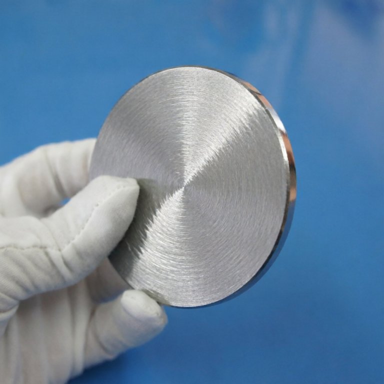
Magnetron sputtering is one of the most widely used industrial methods for AZO deposition. This technique involves bombarding a target material (typically ZnO:Al₂O₃ composite) with energetic ions in a vacuum chamber, causing atoms to be ejected and deposited onto a substrate. Sputtering offers excellent control over film thickness, uniformity, and doping concentration [8].
Recent advancements in sputtering technology have enabled the deposition of high-quality AZO films on flexible polymer substrates. For example, researchers have achieved resistivity of approximately 2.65 × 10⁻³ Ω·cm with optical bandgap of 3.2 eV on polycarbonate substrates using magnetron sputtering [9]. The technique allows for room-temperature deposition, making it compatible with temperature-sensitive substrates.
3.2 Atomic Layer Deposition (ALD)
Atomic layer deposition has emerged as a promising technique for AZO thin films due to its exceptional thickness control, conformality, and uniformity. ALD operates through sequential, self-limiting surface reactions, enabling precise control at the atomic level [10].
Studies have shown that ALD-grown AZO films deposited at 150°C with Zn:Al cycle ratios of 20:2 can achieve resistivity of 2.14 × 10⁻³ Ω·cm with high optical transmittance [11]. The conformal nature of ALD makes it particularly suitable for coating complex three-dimensional structures and high-aspect-ratio features.
3.3 Pulsed Laser Deposition (PLD)
Pulsed laser deposition utilizes high-power laser pulses to ablate material from a target, creating a plasma plume that deposits onto a substrate. PLD offers excellent stoichiometric transfer from target to film and allows for deposition at relatively low temperatures [12].
Research has demonstrated that PLD can produce highly conductive AZO films on flexible polyethylene terephthalate (PET) substrates at room temperature, achieving resistivity of ~6.6 × 10⁻⁴ Ω·cm with high transparency [13]. This makes PLD particularly valuable for flexible electronics applications.
3.4 Sol-Gel Deposition
The sol-gel method involves the preparation of a precursor solution containing zinc and aluminum compounds, which is then deposited onto substrates through techniques such as spin-coating or dip-coating, followed by thermal treatment to form the crystalline film [14].
Sol-gel derived AZO films have shown excellent NO₂ sensing properties, with response and recovery times that can be optimized through aluminum doping concentration [15]. While sol-gel typically produces films with higher resistivity than vacuum-based methods, it offers advantages in terms of cost, scalability, and compatibility with large-area substrates.
4. Key Properties and Performance Metrics
4.1 Electrical Properties
The electrical conductivity of AZO films is primarily determined by carrier concentration and mobility. Optimal aluminum doping concentrations typically range from 1-3 atomic percent, beyond which increased defect scattering can reduce mobility. High-quality AZO films can achieve carrier concentrations exceeding 10²⁰ cm⁻³ and mobilities of 20-40 cm²/V·s [16].
4.2 Optical Properties
AZO maintains high optical transparency in the visible spectrum (typically 80-90%) while exhibiting strong absorption in the ultraviolet region. The optical bandgap can be tuned through doping concentration, typically ranging from 3.2 to 3.8 eV. The Burstein-Moss effect—bandgap widening due to increased carrier concentration—is commonly observed in heavily doped AZO films [17].
4.3 Structural Characteristics
AZO typically crystallizes in the hexagonal wurtzite structure of ZnO, with aluminum atoms substituting for zinc in the lattice. The degree of crystallinity, grain size, and preferred orientation significantly influence both electrical and optical properties. Films with larger grain sizes generally exhibit higher carrier mobility due to reduced grain boundary scattering [18].
5. Applications of AZO Thin Films
5.1 Photovoltaic Devices
AZO serves as an excellent transparent front electrode for thin-film solar cells, including silicon-based, CIGS (copper indium gallium selenide), and perovskite solar cells. Its combination of high transparency and conductivity maximizes light absorption while minimizing resistive losses [19].
5.2 Display Technology
In liquid crystal displays (LCDs), organic light-emitting diodes (OLEDs), and touch panels, AZO provides the necessary transparent conductive layer for electrode functionality. Recent studies have shown that atomic-layer-deposited AZO can outperform ITO in polymer solar cells, demonstrating its potential for next-generation display applications [20].
5.3 Transparent Heat Mirrors
AZO’s combination of high visible transmittance and high infrared reflectance makes it suitable for energy-efficient window coatings. These “low-emissivity” coatings allow visible light transmission while reflecting infrared radiation, reducing heating and cooling energy requirements in buildings [21].
5.4 Gas Sensors
The surface properties and electrical conductivity of AZO make it highly sensitive to various gases, particularly oxidizing gases like NO₂ and O₃. The change in electrical resistance upon gas adsorption enables precise gas detection and monitoring [22].
5.5 Flexible and Wearable Electronics
The compatibility of AZO deposition with flexible polymer substrates enables its use in emerging applications such as flexible displays, wearable sensors, and rollable electronic devices. Room-temperature deposition techniques like sputtering and PLD are particularly valuable for these applications [23].
6. Challenges and Future Directions
Despite its advantages, several challenges remain in the widespread adoption of AZO:
- Long-term Stability: While AZO exhibits good thermal stability, its long-term environmental stability, particularly in humid conditions, requires further improvement through encapsulation or surface passivation techniques.
- Contact Resistance: Achieving low-resistance ohmic contacts to AZO remains challenging for some applications, requiring optimization of interface engineering and contact materials.
- Large-Area Uniformity: Maintaining consistent properties across large substrate areas is crucial for industrial applications and requires advanced deposition control systems.
- P-Type Doping: Developing reliable p-type AZO would enable transparent p-n junctions and expand application possibilities in transparent electronics.
Future research directions include the development of hybrid AZO composites with other materials (such as silver nanowires or graphene) to further enhance conductivity, exploration of novel deposition techniques for improved film quality, and optimization of doping strategies for specific applications.
7. Conclusion
Aluminum doped zinc oxide represents a transformative material in thin film technology, offering a compelling combination of optical transparency, electrical conductivity, cost-effectiveness, and environmental sustainability. Through continuous advancements in deposition techniques and material engineering, AZO has evolved from a promising alternative to ITO into a high-performance material capable of meeting the demanding requirements of modern optoelectronic devices.
The versatility of AZO deposition methods—from industrial-scale sputtering to precision ALD—enables tailored properties for specific applications, from large-area photovoltaic panels to nanoscale electronic devices. As research continues to address remaining challenges and explore new applications, AZO is poised to play an increasingly important role in the development of next-generation transparent electronics, sustainable energy technologies, and advanced sensing systems.
The ongoing optimization of AZO thin films represents not just a material substitution, but a fundamental advancement in transparent conductive technology that aligns with broader trends toward sustainable, cost-effective, and high-performance electronic materials.
8. References
[1] Tseng, M.-C.; Wuu, D.-S.; Chen, C.-L.; Lee, H.-Y.; Chien, C.-Y.; Liu, P.-L.; Horng, R.-H. Characteristics of Atomic Layer Deposition–Grown Zinc Oxide Thin Film with and without Aluminum. Applied Surface Science 2019, 491, 535–543. DOI: 10.1016/j.apsusc.2019.06.055
[2] Nimbalkar, A. R.; Patil, N. B.; Ganbavle, V. V.; Mohite, S. V.; Madhale, K. V.; Patil, M. G. Sol-Gel Derived Aluminium Doped Zinc Oxide Thin Films: A View of Aluminium Doping Effect on Physicochemical and NO2 Sensing Properties. Journal of Alloys and Compounds 2019, 775, 466–473. DOI: 10.1016/j.jallcom.2018.10.144
[3] Wong, L. M.; Chiam, S. Y.; Chim, W. K.; Pan, J. S.; Wang, S. J. Highly Conductive and Transparent Aluminum-Doped Zinc Oxide Thin Films Deposited on Polyethylene Terephthalate Substrates by Pulsed Laser Deposition. Thin Solid Films 2013, 545, 285–290. DOI: 10.1016/j.tsf.2013.08.069
[4] Chen, L.; Chen, X.; Zhou, Z.; Guo, S.; Zhao, Y.; Zhang, X. Studies on Morphology, Electrical and Optical Characteristics of Al-Doped ZnO Thin Films Grown by Atomic Layer Deposition. Journal of Semiconductors 2018, 39 (3), 033004. DOI: 10.1088/1674-4926/39/3/033004
[5] Kan, Z.; Wang, Z.; Firdaus, Y.; Babics, M.; Alshareef, H. N.; Beaujuge, P. M. Atomic-Layer-Deposited AZO Outperforms ITO in High-Efficiency Polymer Solar Cells. Journal of Materials Chemistry A 2018, 6 (22), 10176–10183. DOI: 10.1039/c8ta02841a
[6] Stadler, A. Transparent Conducting Oxides—An Up-To-Date Overview. Materials 2012, 5 (4), 661–683. DOI: 10.3390/ma5040661
[7] Sathish; Shaik, H.; Kumar, K. N.; Jafri, R. I.; Reddy G V, A.; Sattar, S. A. ZnO:Al Thin Films from (Al2O3)x(ZnO)(1-x) Powder Targets by Magnetron Sputtering. Ceramics International 2021, 47 (11), 14997–15004. DOI: 10.1016/j.ceramint.2021.02.037
[8] Eshaghi, A.; Hajkarimi, M. Optical and Electrical Properties of Aluminum Zinc Oxide (AZO) Nanostructured Thin Film Deposited on Polycarbonate Substrate. Optik 2014, 125 (19), 5746–5749. DOI: 10.1016/j.ijleo.2014.07.056
For more information about AZO sputtering target specifications and availability, visit the Aluminum Doped Zinc Oxide Sputtering Targets product page at AtoZmat.
AtoZmat —— Advanced Materials from A to Z.