Abstract
Aluminum sputtering targets are specialized materials used in physical vapor deposition (PVD) processes to create thin aluminum films with precise thickness, composition, and properties. These targets, typically manufactured from high-purity aluminum or aluminum alloys, serve as the source material in sputtering systems where they are bombarded with energetic ions, causing aluminum atoms to be ejected and deposited onto substrates. This article provides a comprehensive overview of aluminum sputtering targets, including their manufacturing, properties, and diverse applications in semiconductor fabrication, optical coatings, microelectronics, and advanced materials science.
Table of Contents
- What are Aluminum Sputtering Targets
- Manufacturing and Properties of Aluminum Sputtering Targets
- Sputtering Processes for Aluminum Deposition
- Properties of Aluminum Thin Films
- Applications of Aluminum Thin Films
- Recent Advances and Future Trends
- Conclusion
- References
1. What are Aluminum Sputtering Targets
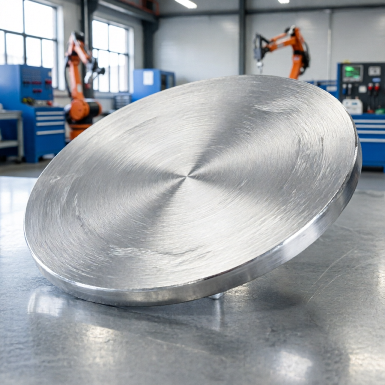
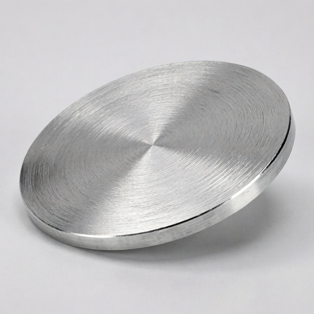
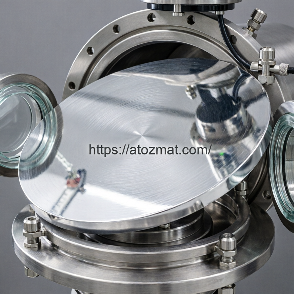
Aluminum sputtering targets are solid materials, usually in disc or rectangular form, composed of high-purity aluminum or aluminum alloys that serve as the source material in sputtering deposition systems. These targets are fundamental components in physical vapor deposition (PVD) processes, particularly magnetron sputtering, which has become the dominant method for depositing aluminum thin films in industrial applications [1].
The significance of aluminum as a sputtering target material stems from its unique combination of properties: excellent electrical conductivity, high reflectivity, good thermal conductivity, and the ability to form a protective oxide layer. Pure aluminum films find extensive applications in optical, microelectronics, telecommunications, and construction industries due to their superior properties including high conductance, low resistivity, high reflectance, better adhesion, and resistance to oxidation and corrosion [1].
2. Manufacturing and Properties of Aluminum Sputtering Targets
2.1 Purity Requirements and Manufacturing Processes
The manufacturing of aluminum sputtering targets requires extreme purity levels, typically exceeding 99.995% (4N5) for semiconductor applications. Ultra-high purity aluminum (>99.999%) is essential for minimizing alpha particle emissions that can cause “soft errors” in integrated circuits [5]. The analysis of ultra-pure aluminum presents unique analytical challenges due to the very low concentration levels of impurities, requiring sophisticated techniques such as glow discharge mass spectroscopy, neutron activation, and inductively coupled plasma optical emission spectroscopy [5].
Target manufacturing involves several critical steps:
- Purification: Multiple purification processes including fractional crystallization, zone refining, and electrolytic refining
- Melting and Casting: Controlled melting in vacuum or inert atmosphere to prevent contamination
- Forming: Hot and cold working processes including rolling, forging, and extrusion
- Machining: Precision machining to achieve required dimensions and surface finish
- Bonding: Attachment to backing plates for efficient heat dissipation during sputtering
2.2 Microstructural Considerations
The microstructure of aluminum sputtering targets significantly influences the properties of deposited films. Research has shown that target microstructure, particularly the amount and distribution of second-phase precipitates, impacts film properties such as resistivity, resistance ratio, reflectivity, and silicon nodule formation [2]. For aluminum alloy targets containing silicon or copper, the distribution of Al₂Cu and Si second-phase precipitates is critical for achieving consistent film properties.
Key Finding: Interestingly, while second-phase content affects film properties, target grain size has been found to have minimal effect on the characteristics of sputtered aluminum films [2]. This understanding has guided target manufacturing toward optimizing precipitate distribution rather than focusing solely on grain refinement.
2.3 Alloy Compositions
Aluminum sputtering targets are often alloyed with other elements to enhance specific properties:
| Alloy Type | Composition | Application |
|---|---|---|
| Al-Si | 0.5-2% Si | Prevents “spiking” in semiconductor applications |
| Al-Cu | 0.5-4% Cu | Reduces electromigration in interconnects |
| Al-Ti | Various | Barrier layers in semiconductor metallization |
| Pure Al | >99.995% | Optical coatings and reflective applications |
3. Sputtering Processes for Aluminum Deposition
3.1 Magnetron Sputtering Fundamentals
Magnetron sputtering is the most widely used technique for aluminum thin film deposition. In this process, a plasma is created in a low-pressure argon atmosphere, and ions are accelerated toward the aluminum target by an applied electric field. The impact of these energetic ions causes aluminum atoms to be ejected from the target surface through momentum transfer, a phenomenon known as sputtering [7].
The sputtered aluminum atoms travel through the vacuum chamber and condense on substrates positioned opposite the target. The process parameters that control film properties include:
- Sputtering power: Typically 1-10 kW for industrial systems
- Process pressure: Usually 0.1-10 Pa
- Substrate temperature: Ranging from room temperature to 500°C
- Target-to-substrate distance: Typically 5-15 cm
- Gas composition: Pure argon for metallic films; argon-oxygen or argon-nitrogen mixtures for reactive sputtering
3.2 Reactive Sputtering for Aluminum Compounds
Reactive sputtering enables the deposition of aluminum compound films such as aluminum oxide (Al₂O₃) and aluminum nitride (AlN). In this process, aluminum is sputtered in the presence of reactive gases (oxygen or nitrogen), resulting in compound formation either at the target surface, in the gas phase, or on the substrate [3].
For aluminum oxide deposition, researchers have achieved deposition rates of 215 nm/min for stress-free, transparent films, representing approximately 77% of the deposition rate for metallic aluminum [3]. The deposition process is typically controlled by monitoring target voltage to obtain stoichiometric thin films with optimal properties.
3.3 Process Optimization and Challenges
Several challenges must be addressed in aluminum sputtering processes:
Target Poisoning: In reactive sputtering, the formation of dielectric compounds on the target surface (target poisoning) reduces deposition rates significantly. The sputtering yield of aluminum oxide is much lower than that of metallic aluminum, leading to deposition rates that can be 7-10 times lower than for pure metal deposition [4]. Advanced techniques such as pulsed magnetron sputtering with automated process stabilization have been developed to maintain operation in the transition mode between metallic and poisoned states, optimizing deposition rates [4].
Gas Purity Effects: The purity of sputtering gases significantly affects film properties. Research has shown that gas purity impacts the reflectance and resistivity of magnetron-sputtered aluminum and its alloys, with higher purity gases yielding films with better optical and electrical properties [8].
Deposition Rate Optimization: For high-rate deposition of aluminum films, operation parameters must be carefully optimized. Studies have demonstrated that specific magnetron diode configurations and operating conditions can maximize deposition rates while maintaining film quality [7].
4. Properties of Aluminum Thin Films
4.1 Electrical Properties
Aluminum thin films exhibit excellent electrical conductivity, with bulk resistivity of approximately 2.65 μΩ·cm for pure aluminum. The resistivity of sputtered films is typically slightly higher due to grain boundary scattering and impurity incorporation. Film resistivity depends on several factors including deposition parameters, substrate temperature, and post-deposition treatments [1].
For semiconductor applications, aluminum films with low resistivity are essential for minimizing RC delays in interconnects. The addition of copper to aluminum reduces electromigration susceptibility while maintaining acceptable conductivity.
4.2 Optical Properties
Aluminum is widely used for optical coatings due to its high reflectivity across a broad spectral range. Freshly deposited aluminum films can achieve reflectivities exceeding 90% in the visible spectrum. However, aluminum readily forms a native oxide layer (Al₂O₃) that affects optical properties. This oxide layer, typically 2-5 nm thick, can be controlled to tailor optical characteristics for specific applications [1].
The specular reflectivity of aluminum films is influenced by deposition parameters, with smoother films exhibiting higher specular reflectivity. Substrate temperature, deposition rate, and process pressure all affect film morphology and consequently optical properties.
4.3 Mechanical Properties
Aluminum thin films possess good mechanical properties including:
- Adhesion: Excellent adhesion to various substrates including silicon, glass, and polymers
- Stress: Intrinsic stress can be controlled through deposition parameters and post-deposition annealing
- Hardness: Pure aluminum films have moderate hardness; aluminum oxide films exhibit significantly higher hardness values
The mechanical properties of aluminum films are crucial for applications requiring durability and wear resistance, such as protective coatings and microelectromechanical systems (MEMS).
4.4 Thermal Properties
Aluminum’s high thermal conductivity (approximately 237 W/m·K for bulk material) makes it suitable for thermal management applications. Thin aluminum films can serve as heat spreaders in electronic devices, helping to dissipate heat from active components.
5. Applications of Aluminum Thin Films
5.1 Semiconductor Industry
Aluminum sputtering targets find their most significant application in semiconductor manufacturing, where they are used for metallization processes. Key applications include:
Interconnects: Aluminum and aluminum alloys (primarily Al-Si and Al-Si-Cu) serve as interconnect materials in integrated circuits, providing electrical connections between transistors and other circuit elements. The transition to copper interconnects in advanced nodes has reduced aluminum usage in front-end applications, but aluminum remains important for certain applications and in packaging [2].
Barrier Layers: Aluminum-containing compounds such as TiAl₃ and TiAlN serve as diffusion barriers between copper interconnects and dielectric materials, preventing copper migration that can degrade device performance.
Reflective Coatings: Aluminum films provide reflective surfaces for photolithography masks and certain optical elements in semiconductor manufacturing equipment.
5.2 Optical Coatings
Aluminum’s high reflectivity makes it ideal for optical applications:
- Mirrors and Reflectors: Astronomical telescopes, laser cavities, and lighting systems
- Decorative Coatings: Automotive trim, packaging, and consumer products
- Solar Reflectors: Concentrated solar power systems and building insulation
For optical applications, aluminum is often protected with dielectric overcoats (such as SiO₂ or MgF₂) to prevent oxidation and enhance durability.
5.3 Microelectronics and Displays
Beyond semiconductor interconnects, aluminum films are used in:
- Thin-film transistors: Aluminum gates and electrodes in display technologies
- MEMS devices: Structural layers and electrical contacts
- RF components: Inductors, capacitors, and transmission lines
- Transparent conductive oxides: Aluminum-doped zinc oxide (AZO) as an alternative to indium tin oxide (ITO)
5.4 Protective and Functional Coatings
Aluminum and aluminum compound films provide:
- Corrosion protection: Aluminum oxide coatings on steel and other metals
- Wear resistance: Hard aluminum oxide coatings on cutting tools and mechanical components
- Gas barrier layers: Aluminum oxide films on flexible packaging materials
- Biomedical coatings: Aluminum oxide for biocompatible surfaces on implants
6. Recent Advances and Future Trends
6.1 High-Power Pulsed Magnetron Sputtering (HPPMS)
Recent developments in HPPMS technology have enabled improved aluminum nitride (AlN) thin film deposition. Research has identified optimal target sputtering modes that enhance film quality while maintaining reasonable deposition rates [6]. HPPMS produces highly ionized plasmas that allow better control over film microstructure and properties, particularly for compound films like AlN used in piezoelectric applications.
6.2 Process Control and Automation
Advanced process control systems utilizing real-time monitoring of electrical parameters have improved the stability and reproducibility of aluminum sputtering processes. Automated stabilizers driven by power supply parameters enable operation in the transition mode between metallic and poisoned states, optimizing deposition rates for reactive processes [4].
6.3 Novel Aluminum Alloys and Compounds
Research continues on developing new aluminum-based materials for sputtering targets:
- Aluminum scandium nitride: For enhanced piezoelectric properties in MEMS applications
- Aluminum-containing high-k dielectrics: For advanced semiconductor devices
- Nanostructured aluminum coatings: For plasmonic and sensing applications
6.4 Sustainability and Recycling
With increasing emphasis on sustainable manufacturing, efforts are underway to improve the recyclability of aluminum sputtering targets. Target reclamation processes that allow multiple uses of backing plates and recycling of target materials are becoming more prevalent in the industry.
7. Conclusion
Aluminum sputtering targets are essential components in thin film deposition processes, enabling the production of aluminum and aluminum compound films with precisely controlled properties. The manufacturing of these targets requires extreme purity levels and careful control of microstructure to ensure consistent film properties. Magnetron sputtering, particularly in reactive modes for compound deposition, remains the dominant technology for aluminum thin film deposition.
The applications of aluminum thin films span multiple industries, with semiconductor manufacturing representing the most significant market. Ongoing research focuses on improving deposition rates, enhancing film properties, and developing new aluminum-based materials for emerging applications. As thin film technologies continue to advance, aluminum sputtering targets will remain critical materials enabling innovations in electronics, optics, energy, and advanced manufacturing.
The future of aluminum sputtering targets lies in the development of more sophisticated alloys, improved process control systems, and sustainable manufacturing practices that address the evolving needs of high-technology industries while minimizing environmental impact.
8. References
[1] Mwema, F. M.; Oladijo, O. P.; Akinlabi, S. A.; Akinlabi, E. T. Properties of Physically Deposited Thin Aluminium Film Coatings: A Review. Journal of Alloys and Compounds 2018, 747, 306–323. DOI: 10.1016/j.jallcom.2018.03.006
[2] Bailey, R. S. Effects of Target Microstructure on Aluminum Alloy Sputtered Thin Film Properties. Journal of Vacuum Science & Technology A: Vacuum, Surfaces, and Films 1992, 10 (4), 1701–1705. DOI: 10.1116/1.577773
[3] Koski, K.; Hölsä, J.; Juliet, P. Deposition of Aluminium Oxide Thin Films by Reactive Magnetron Sputtering. Surface and Coatings Technology 1999, 116–119, 716–720. DOI: 10.1016/s0257-8972(99)00087-0
[4] Wiatrowski, A.; Patela, S.; Kunicki, P.; Posadowski, W. Effective Reactive Pulsed Magnetron Sputtering of Aluminium Oxide – Properties of Films Deposited Utilizing Automated Process Stabilizer. Vacuum 2016, 134, 54–62. DOI: 10.1016/j.vacuum.2016.09.021
[5] Genna, J. L. Consideration of Accuracy in the Analysis of Ultra Pure Aluminum. Journal of Crystal Growth 1988, 89 (1), 62–67. DOI: 10.1016/0022-0248(88)90072-3
[6] Ma, D. L.; Liu, H. Y.; Deng, Q. Y.; Yang, W. M.; Silins, K.; Huang, N.; Leng, Y. X. Optimal Target Sputtering Mode for Aluminum Nitride Thin Film Deposition by High Power Pulsed Magnetron Sputtering. Vacuum 2019, 160, 410–417. DOI: 10.1016/j.vacuum.2018.11.058
[7] Sidelev, D. V.; Grudinin, V. A. Operation Parameters of Magnetron Diode for High-Rate Deposition of Aluminum Films. Journal of Physics: Conference Series 2018, 1115, 032020. DOI: 10.1088/1742-6596/1115/3/032020
[8] Nyaiesh, A.; Holland, L. The Effect of Gas Purity on the Reflectance and Resistivity of Magnetron Sputtered Aluminium and Its Alloys. Vacuum 1982, 32 (10–11), 585–590. DOI: 10.1016/0042-207x(82)93845-3
Product Information
AtoZmat —— Advanced Materials from A to Z.
High-purity aluminum sputtering targets in standard and custom sizes are available from AtoZmat. For detailed specifications, pricing, and ordering information, visit: