Lead arsenide (PbAs) sputtering targets sit in a technically demanding corner of thin-film materials engineering. Pb-As compounds are relevant to narrow-gap electronic behavior, infrared-responsive materials research, and exploratory semimetallic and thermoelectric systems, but they are also difficult to process cleanly and reproducibly. For engineers and researchers, the main challenge is not simply depositing a film; it is preserving composition while managing arsenic volatility, lead-rich defect formation, phase selectivity, and contamination introduced during target fabrication or sputtering.
This makes target quality unusually important. In compound semiconductor sputtering, the target is not only the source material but also a strong determinant of transfer fidelity, plasma stability, particulate generation, and ultimately film stoichiometry. For PbAs, small deviations in Pb:As ratio can shift carrier density, defect chemistry, grain structure, and optical response enough to move a film out of its intended operating window.
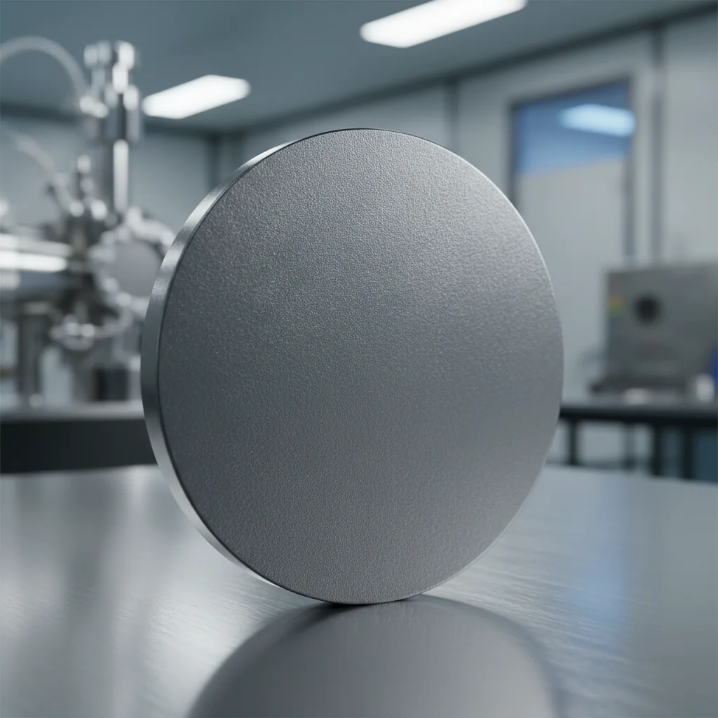
Close-up view of Lead Arsenide Sputtering Targets (PbAs Sputtering Targets) | PbAs-ST
Introduction
PbAs sputtering targets are typically used when a process requires more compositional uniformity and area scalability than can be achieved with evaporation from separate elemental sources. Sputtering offers practical advantages for research-scale multilayers, diffusion barriers, exploratory semiconductor stacks, and alloyed or doped film programs. However, PbAs is not a forgiving target material. The large atomic mass of lead, the chemical sensitivity of arsenic, and the tendency of arsenic-containing films to lose stoichiometry under energetic deposition conditions all complicate process development.
For this reason, a serious evaluation of PbAs targets should focus on density, phase purity, oxygen content, microstructural integrity, and response under sputtering power rather than on nominal composition alone. AtoZMat lists PbAs sputtering targets for thin-film work, and for technical users the more important question is how such a target will behave in a real deposition environment: whether it sputters uniformly, whether it maintains composition under extended runs, and whether the resulting films can be crystallized without severe arsenic loss.
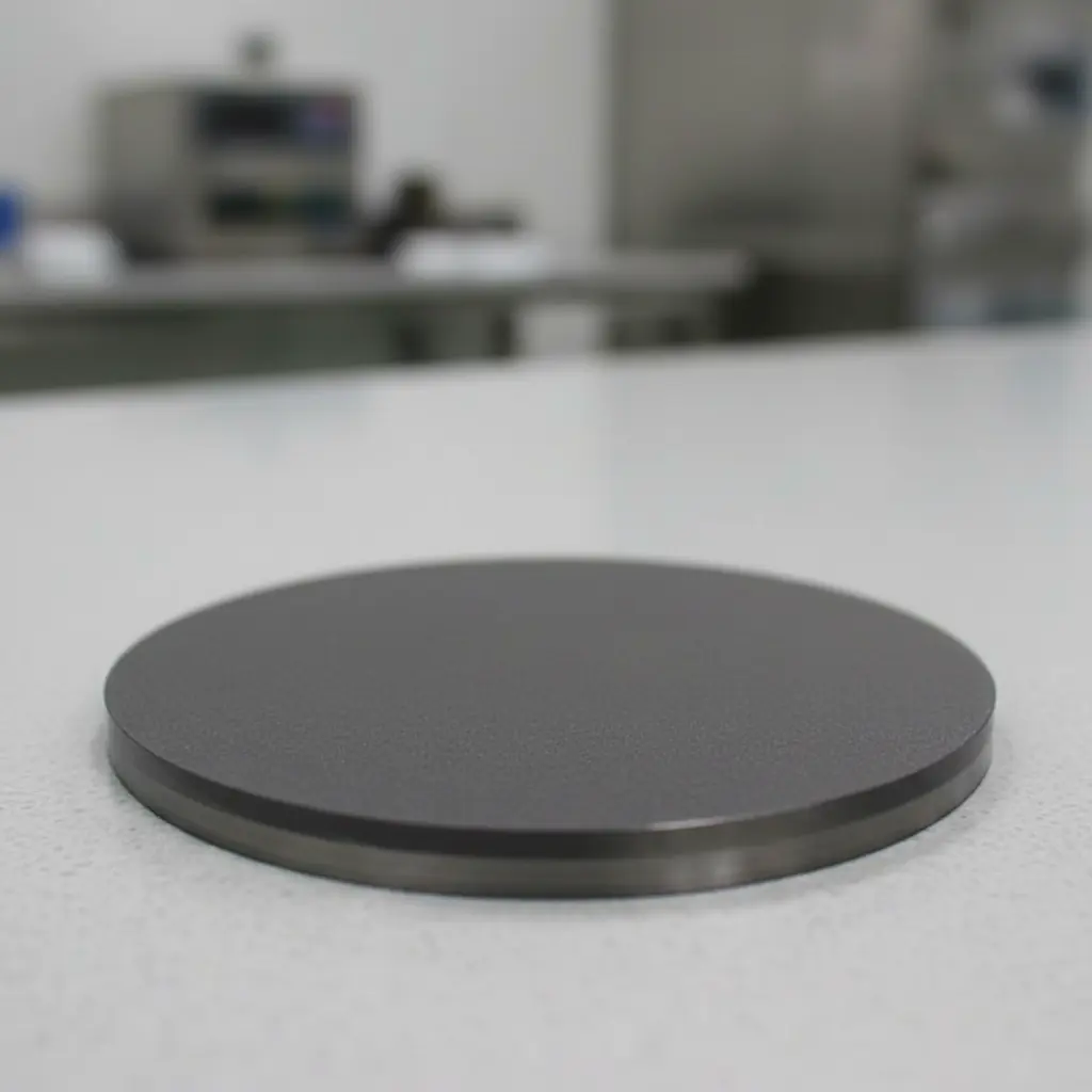
Research laboratory application context for Lead Arsenide Sputtering Targets (PbAs Sputtering Targets) | PbAs-ST
Technical Background
Lead-arsenic materials belong to a broader class of heavy-element semiconducting and semimetallic systems in which electronic structure is highly sensitive to composition, bonding environment, and crystalline order. In published work on Pb-As compounds and related lead pnictide systems, researchers have repeatedly found that electronic properties can change sharply with small composition shifts, secondary-phase formation, or vacancy concentration. In thin films, this sensitivity is amplified because non-equilibrium deposition can freeze in point defects, local segregation, and nanocrystalline disorder.
From a sputtering perspective, several material features matter:
Arsenic volatility: arsenic loss during deposition or post-deposition heating can drive the film lead-rich, promoting metallic conduction, altered optical absorption, or phase decomposition.
Mass asymmetry: the large mass difference between Pb and As affects sputter yield balance and angular distribution of ejected species.
Target brittleness: many compound targets are susceptible to cracking, edge chipping, or localized overheating if density and bonding quality are poor.
Surface oxidation: oxygen-bearing contamination on the target surface can be transferred into the film, where it may act as a deep defect source or nucleation site for non-ideal phases.
Dense, homogeneous targets are therefore preferred. In many compound sputtering systems, moving from ~90-92% of theoretical density to >97-98% can noticeably reduce arcing, particle generation, and erosion nonuniformity. That trend is especially relevant for fragile or composition-sensitive targets such as PbAs.
Processing Behavior and Deposition Considerations
Target quality and purity
For PbAs, purity is not a cosmetic specification. Metallic impurities can alter carrier concentration directly, while oxygen, sulfur, and carbon contamination can broaden X-ray diffraction peaks, degrade mobility, and complicate interpretation of optical data. In narrow-gap and semimetal-adjacent materials, impurity levels in the tens to low hundreds of ppm can become electrically significant. For researchers studying intrinsic transport or optical transitions, low impurity burden is therefore essential.
Microstructural uniformity inside the target also matters. If the target contains local lead-rich or arsenic-rich regions, the erosion track can evolve during sputtering and shift the deposited composition over time. This is often seen as a drift in sheet resistance, refractive index, or XPS-measured stoichiometry over long runs.
Sputtering mode: DC vs. RF
The preferred power mode depends on the electrical behavior of the target and the process objective. If the target exhibits sufficiently conductive behavior, DC magnetron sputtering may be possible and offers higher deposition rates. RF sputtering is often used when target conductivity is limited, when insulating surface films form, or when tighter control is needed during exploratory process development. In practice, many compound semiconductor programs start under RF conditions because it is more forgiving of surface chemistry variations and less prone to unstable discharge when native oxide or arsenic-rich surface regions are present.
Working gas and pressure
Argon is the standard sputtering gas, but pressure selection has a strong effect on film composition and density. Lower pressures generally increase adatom energy and film density but can also intensify preferential resputtering of the more volatile or lighter species at the substrate. Higher pressures improve scattering and can moderate energetic damage, but they often reduce density and increase columnar growth. For PbAs films, a moderate-pressure window is usually preferred to balance transfer fidelity and microstructural quality.
In many compound target systems, process windows around 2-8 mTorr are investigated first. Within this range, it is common to observe measurable composition drift with pressure changes of only a few mTorr, especially when substrate bias is applied.
Substrate temperature and arsenic retention
Substrate temperature is one of the most consequential variables. Higher temperature generally improves surface diffusion, grain growth, and crystallinity, but it also raises the risk of arsenic loss. In lead-arsenic thin films, this trade-off can be severe. Reports on arsenic-containing sputtered semiconductors frequently show that temperatures above roughly 200-300 °C can begin to shift composition if the arsenic chemical potential is not otherwise stabilized. Exact thresholds depend on chamber pressure, deposition rate, film thickness, and whether a capping or overpressure strategy is used.
For many research programs, a practical route is:
deposit near room temperature or at modest heating to preserve stoichiometry,
then use a controlled post-deposition anneal, sometimes with a cap layer or confined ambient,
and verify composition afterward by XPS, EDS, or RBS rather than assuming the target composition transferred directly.
Composition transfer and preferential sputtering
Compound target sputtering rarely guarantees exact stoichiometric transfer. Preferential sputtering, resputtering at the substrate, and differential sticking can all shift film composition. In PbAs systems, arsenic deficiency is a recurring risk. Even a deviation of 1-3 at.% can significantly alter free carrier concentration or move the material into a multiphase regime. For device-oriented work, that is a large error.
Because of this, composition should be tracked as a process output, not treated as an assumed constant. Good practice includes correlating target age, erosion profile, chamber history, pressure, and substrate temperature with measured film stoichiometry. In research settings, this often reveals that the target itself is only one part of the composition-control problem.
Film Microstructure, Stability, and Performance
Crystallinity and grain development
As-deposited PbAs films may be amorphous, nanocrystalline, or weakly textured depending on thermal budget and deposition energy. Improved crystallinity often lowers resistivity scatter and sharpens optical features, but excessive thermal treatment can trigger arsenic depletion, roughening, or secondary-phase formation. Grain size in sputtered compound semiconductor films frequently moves from the low-nanometer regime in cold deposition toward tens of nanometers after annealing, with accompanying changes in mobility and optical absorption edge.
For performance-sensitive films, XRD peak width, AFM roughness, and cross-sectional SEM are all useful. A film that appears compositionally correct by EDS may still underperform because it contains nanovoids, high-angle grain boundaries, or segregated Pb-rich regions below conventional compositional detection limits.
Electrical behavior
Electronic performance in PbAs films is closely tied to point defects and stoichiometry. Lead-rich growth often increases carrier density and can push behavior toward more metallic transport, while arsenic-rich or oxygen-contaminated growth may increase defect scattering and destabilize reproducibility. In narrow-gap materials and semimetal-like compounds, room-temperature resistivity can vary by orders of magnitude across nominally similar samples if composition control is poor.
This is one reason why sputtered PbAs is often more useful for comparative materials research than for immediate device deployment unless the process has been carefully tuned. Hall measurements, temperature-dependent resistivity, and Seebeck data can be more revealing than simple room-temperature sheet resistance when screening process changes.
Optical and infrared relevance
Lead-containing pnictide and chalcogenide systems are often studied because of their narrow electronic features and potential relevance to infrared detection, thermal sensing, and specialized electronic structures. In thin films, however, optical response depends not only on nominal chemistry but on thickness uniformity, grain-boundary density, and free-carrier absorption from off-stoichiometry. A film with acceptable XRD data can still show broadened or shifted optical behavior if the defect population is high.
Applications and Engineering Context
PbAs sputtering targets are most relevant in research and specialty thin-film programs rather than broad commodity coating markets. The main application contexts include:
Narrow-gap semiconductor studies: exploratory electronic and optoelectronic films where composition-sensitive band structure is of interest.
Infrared-responsive thin films: materials stacks for detector research, thermal sensing concepts, or spectral-response studies.
Thermoelectric and transport research: heavy-element compounds are often screened for unusual carrier transport and low thermal conductivity behavior.
Multilayer and heterostructure experiments: sputtering enables integration with diffusion barriers, contacts, cap layers, and substrate-engineering strategies.
Fundamental phase and topological materials research: Pb-As systems and neighboring compositions are of interest where relativistic electronic effects and composition-tuned phases are being investigated.
In these areas, sputtering is attractive because it can produce uniform films over larger areas than many laboratory evaporation setups and can be integrated with standard semiconductor process flows. The trade-off is that composition control must be actively engineered rather than assumed.
Challenges and Trade-Offs
Stoichiometry vs. crystallinity: higher temperature improves crystal quality but increases arsenic loss risk.
Deposition rate vs. film quality: more aggressive power can raise throughput but may increase defect density, resputtering, and roughness.
Target density vs. manufacturing difficulty: very dense compound targets are preferable but harder to produce without cracking or segregation.
Purity vs. cost: electronic-grade impurity control is valuable for transport studies, but not every exploratory program requires the same threshold.
Process simplicity vs. reproducibility: single-step deposition is attractive, yet two-step deposition plus annealing may be more reliable for phase formation.
Another practical challenge is environmental and safety control. Lead and arsenic both require disciplined handling, exhaust management, waste segregation, and maintenance protocols. In sputtering systems, this affects target changeout, shield cleaning, pump maintenance, and post-process analytical sample preparation. For many organizations, EHS readiness becomes part of the real process-selection decision.
Research Directions and Future Opportunities
Current research interest around Pb-As thin films is likely to remain strongest in three areas.
1. Better stoichiometry control in non-equilibrium deposition
There is ongoing value in process strategies that suppress arsenic loss without sacrificing film density. These include lower-damage plasma conditions, pulsed power, carefully tuned substrate bias, capping layers, and short high-temperature anneals rather than long thermal exposure.
2. Interface-engineered heterostructures
As device concepts become more interface-dominated, PbAs films are increasingly relevant as part of multilayer stacks rather than as standalone thick films. In such structures, interdiffusion, contact resistance, and reaction layers can dominate performance. This raises the importance of smooth, low-particle sputtered films and tightly controlled impurity content.
3. Transport and topological-property exploration
Heavy-element arsenides continue to attract attention for unusual band structures, strong spin-orbit coupling effects, and nontrivial transport phenomena. Thin-film sputtering is useful here because it allows strain, thickness, and interface effects to be studied systematically. High-quality targets are a prerequisite for meaningful results, since defect-driven conductivity can easily mask intrinsic behavior.
Conclusion
Lead arsenide sputtering targets are best understood as process-critical inputs for difficult compound film deposition rather than as routine consumables. Their value depends on density, purity, phase uniformity, and the ability to support stable sputtering without composition drift. For PbAs films, the central engineering issue is stoichiometry control under conditions where arsenic volatility and non-equilibrium growth compete directly with crystallinity and performance.
For technical users, successful implementation usually comes from treating target selection, plasma conditions, substrate temperature, and post-deposition thermal history as a coupled system. When that is done well, sputtered PbAs can support serious work in narrow-gap semiconductor research, infrared-active materials development, and advanced transport studies. When it is not, apparently small composition errors can dominate the entire result.