Measuring temperatures above 1500°C presents significant challenges in industrial and research environments. Standard thermocouple materials often fail at extreme temperatures, creating measurement gaps in applications like aerospace testing, advanced materials processing, and high-temperature furnace operations. Tungsten rhenium thermocouple wire addresses this challenge by extending reliable temperature measurement into ranges where conventional sensors cannot operate.
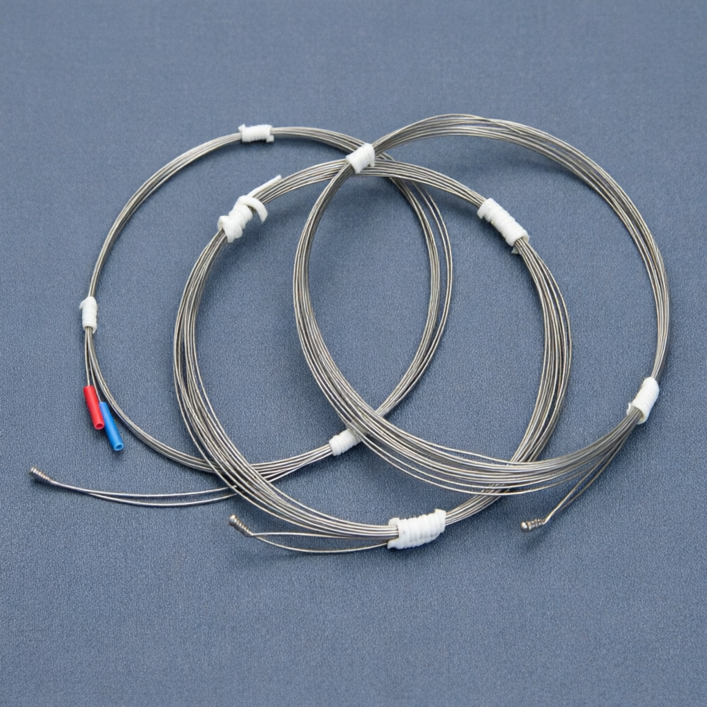
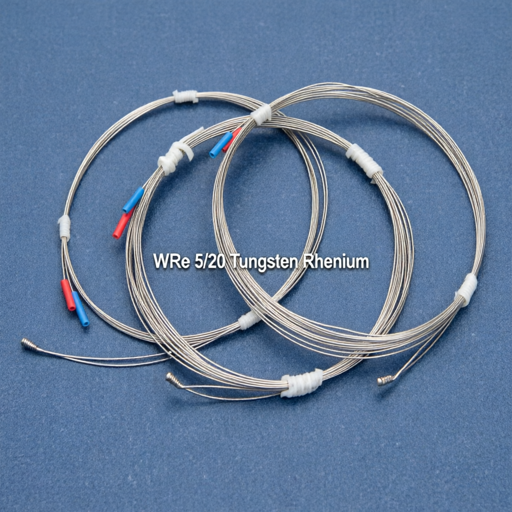
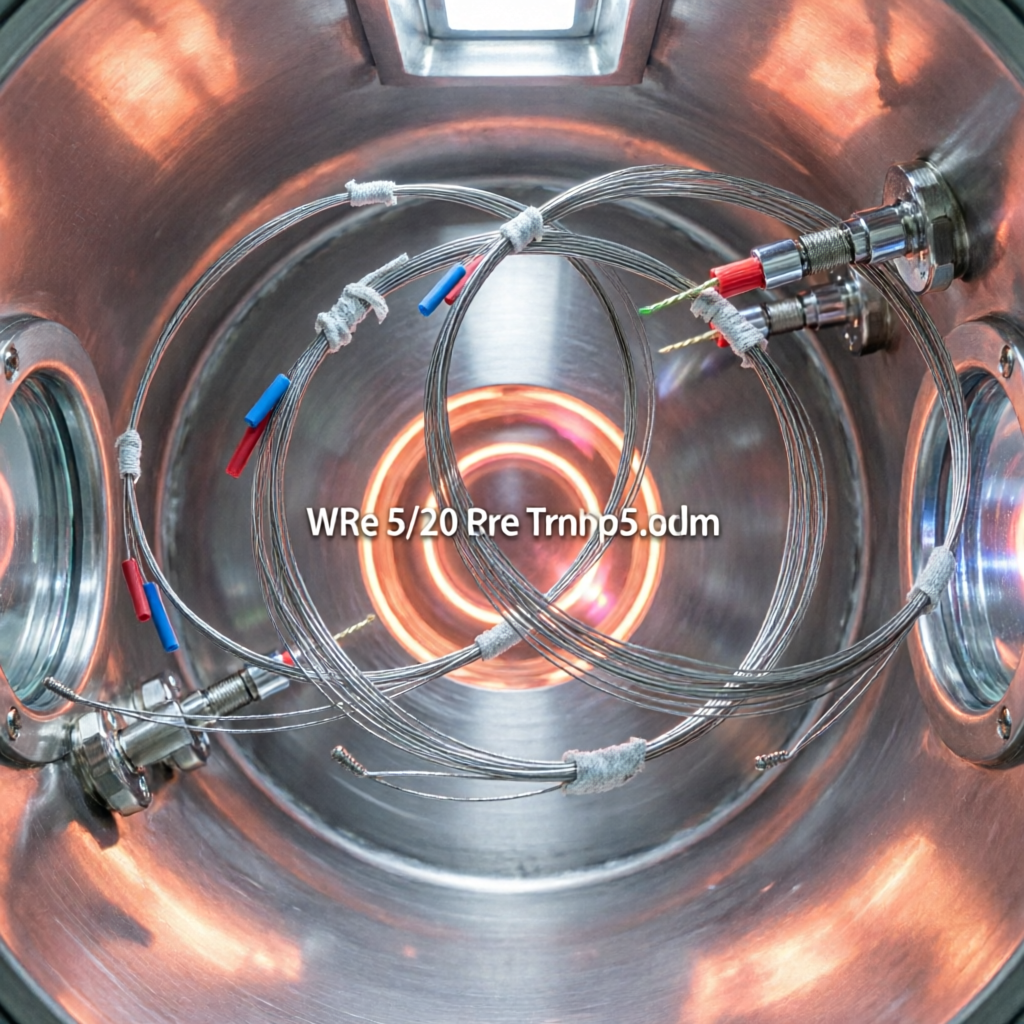
Tungsten rhenium thermocouple wire consists of tungsten-rhenium alloys paired to create a thermoelectric circuit capable of measuring temperatures from approximately 1500°C to 3000°C. The most common pairing combines a low-rhenium alloy leg with a high-rhenium alloy leg. The WRe 5/20 configuration pairs a 5% rhenium alloy (W-5Re) with a 20% rhenium alloy (W-20Re), creating a thermocouple junction that generates measurable voltage differences across extreme temperature gradients.
Other standard pairings include WRe 3/25 and WRe 5/26, each offering slightly different temperature response characteristics and stability profiles. The addition of rhenium to tungsten improves ductility and workability compared to pure tungsten, while maintaining the high melting point necessary for ultra-high temperature service.
Pure tungsten has an extremely high melting point but is brittle and difficult to draw into fine wire. Rhenium addition transforms the material’s mechanical properties without significantly compromising its temperature capability. Low-rhenium alloys (typically 3-5% Re) provide one thermoelectric leg, while high-rhenium alloys (20-26% Re) provide the complementary leg with different thermoelectric characteristics.
This pairing creates sufficient thermoelectric voltage for accurate measurement while both legs maintain structural integrity at temperatures where most metals would melt or oxidize. The specific rhenium percentages in each leg determine the thermocouple’s sensitivity, linearity, and maximum operating temperature.
Primary Applications
Tungsten rhenium thermocouples serve applications where temperature measurement exceeds the capability of platinum-rhodium or base metal thermocouples:
Aerospace and propulsion testing: Engine component testing, combustion research, and thermal protection system evaluation often require temperature measurement above 2000°C in controlled atmospheres or vacuum conditions.
Advanced materials processing: Sintering operations for ceramics, refractory metals, and composite materials frequently operate at temperatures where tungsten rhenium thermocouples provide the only practical measurement option.
Vacuum furnace operations: High-temperature heat treatment, crystal growth, and materials synthesis in vacuum or inert atmospheres benefit from tungsten rhenium’s stability in non-oxidizing environments.
Research and development: Materials science laboratories use tungsten rhenium thermocouples for high-temperature property characterization, phase transition studies, and process development work.
Atmospheric Limitations and Protection Requirements
Tungsten rhenium thermocouples perform best in vacuum, inert gas, or reducing atmospheres. Oxidation becomes a significant concern above approximately 1000°C in air or oxidizing environments. The tungsten component oxidizes readily, leading to rapid degradation and measurement drift.
Engineers typically protect tungsten rhenium thermocouples with ceramic sheaths or operate them in controlled atmospheres. Common protective materials include alumina, magnesia, or specialized refractory ceramics, though sheath selection depends on the specific temperature range and chemical environment. In some high-vacuum applications, bare wire configurations may be acceptable, but contamination and embrittlement risks increase with exposure time.
Wire Diameter and Mechanical Considerations
Tungsten rhenium thermocouple wire is commonly available in diameters ranging from 0.25mm to 1.0mm. Finer wire diameters (0.25mm to 0.5mm) offer faster thermal response and smaller measurement volumes, making them suitable for localized temperature sensing or applications with tight spatial constraints. Larger diameters (0.5mm to 1.0mm) provide greater mechanical strength and longer service life in demanding environments.
Wire diameter selection involves trade-offs between response time, durability, and ease of handling. Finer wires are more fragile during installation and more susceptible to contamination or mechanical damage. Thicker wires withstand handling better but may introduce larger thermal mass effects in small-scale measurements.
Cost Considerations Compared to Platinum-Rhodium
One practical advantage of tungsten rhenium thermocouples is their cost structure relative to platinum-rhodium alternatives. While platinum-rhodium thermocouples (Types R, S, and B) are standard for many high-temperature applications up to approximately 1700°C, their precious metal content makes them expensive, particularly for larger installations or applications requiring multiple measurement points.
Tungsten rhenium thermocouples extend the temperature range beyond platinum-rhodium capability while using less expensive base materials. However, the specialized processing required for tungsten rhenium alloys and the limited number of manufacturers mean these thermocouples are not commodity items. Buyers should expect lead times and pricing that reflect specialized manufacturing rather than off-the-shelf availability.
Calibration and Measurement Accuracy
Tungsten rhenium thermocouples require careful calibration, particularly for precision measurement applications. Standard reference tables exist for common pairings like WRe 5/26 (Type C) and WRe 3/25 (Type D), but individual thermocouple calibration often improves accuracy in critical applications.
Measurement drift can occur over time due to grain growth, contamination, or preferential evaporation of rhenium at extreme temperatures. Engineers working with tungsten rhenium thermocouples typically implement periodic recalibration schedules or use redundant sensors for critical measurements. Drift rates depend heavily on operating temperature, atmosphere, and thermal cycling frequency.
Common Selection Factors
When specifying tungsten rhenium thermocouple wire, engineers typically consider:
Temperature range: Maximum operating temperature determines whether WRe 5/20, WRe 3/25, or WRe 5/26 pairings are most appropriate. Higher rhenium content in the positive leg generally extends upper temperature capability.
Atmosphere compatibility: Vacuum, inert gas, or reducing atmospheres are essential for long-term stability. Oxidizing environments require protective measures or alternative sensor technologies.
Response time requirements: Wire diameter and junction configuration affect thermal response. Exposed junction designs offer faster response than grounded or insulated junctions.
Mechanical durability: Installation environment, vibration exposure, and handling requirements influence wire diameter selection and sheath design.
Measurement accuracy needs: Critical applications may require individual calibration, while less demanding uses can rely on standard reference tables.
Installation and Handling Practices
Tungsten rhenium wire is more brittle than base metal thermocouple wire, requiring careful handling during installation. Sharp bends or mechanical stress can cause wire fracture, particularly with finer diameters. Junction formation typically uses capacitive discharge welding or other specialized techniques rather than conventional soldering.
Contamination control is important during installation. Surface contaminants can affect thermoelectric properties or accelerate degradation at high temperatures. Clean handling practices and proper storage in controlled environments help maintain wire quality before use.
Current Research and Development Directions
Ongoing work in high-temperature sensing continues to explore tungsten rhenium alloy optimization, protective coating development, and alternative junction designs. Research efforts focus on extending service life in challenging atmospheres, improving measurement stability over thermal cycles, and reducing drift rates at extreme temperatures. Some development work examines thin-film thermocouple configurations using tungsten rhenium alloys for surface temperature measurement in aerospace and energy applications.
Practical Sourcing Considerations
Tungsten rhenium thermocouple wire is available from specialized manufacturers serving high-temperature measurement markets. Standard offerings typically include matched pairs of low-rhenium and high-rhenium wire in common diameters, often sold in lengths of 10m, 25m, or 100m. Custom diameters and alloy compositions may be available with longer lead times.
Buyers should verify wire purity specifications, typically 99.95% or higher, and confirm that both legs of the thermocouple pair come from the same production lot to ensure consistent thermoelectric properties. Documentation of alloy composition and calibration data supports quality control and traceability requirements in regulated industries.
Conclusion
Tungsten rhenium thermocouple wire provides essential temperature measurement capability in extreme environments where conventional sensors cannot operate. The WRe 5/20 configuration offers a practical balance of temperature range, cost, and availability for applications between 1500°C and 2800°C in controlled atmospheres. Understanding the material’s atmospheric limitations, mechanical properties, and calibration requirements helps engineers select and implement these specialized sensors effectively in demanding high-temperature applications.
WRe 5/20 Tungsten Rhenium Thermocouple Wire
atozmat supplies WRe 5/20 tungsten rhenium thermocouple wire in standard diameters from 0.25mm to 1.0mm, with purity over 99.95%. Available in 10m, 25m, and 100m lengths.
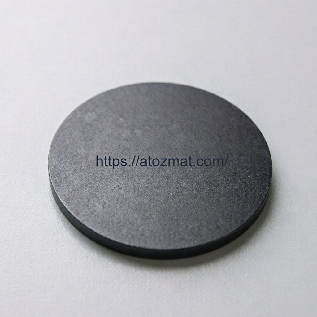
Copper selenide (CuSe2) has emerged as a compelling material in thin film research, particularly for applications requiring tunable electronic properties and earth-abundant composition. As researchers explore alternatives to conventional semiconductor materials, copper selenide sputtering targets have become essential tools for depositing high-quality films in laboratory and pilot-scale environments.
Understanding Copper Selenide as a Thin Film Material
Copper selenide represents a family of copper-selenium compounds with varying stoichiometries, including Cu2Se, CuSe, and CuSe2. The CuSe2 phase specifically exhibits p-type semiconductor behavior with a narrow bandgap, making it attractive for optoelectronic and energy conversion applications. Unlike many traditional thin film materials that rely on rare or toxic elements, copper selenide offers a more sustainable materials profile while maintaining interesting electronic and optical properties.
The material’s crystal structure and phase stability depend heavily on deposition conditions. Researchers working with copper selenide films typically encounter challenges related to stoichiometry control, as the copper-to-selenium ratio can shift during sputtering depending on target composition, power density, and chamber pressure. Films deposited from CuSe2 targets generally show better compositional control compared to co-sputtering approaches, though post-deposition annealing may still be necessary to achieve desired phase purity.
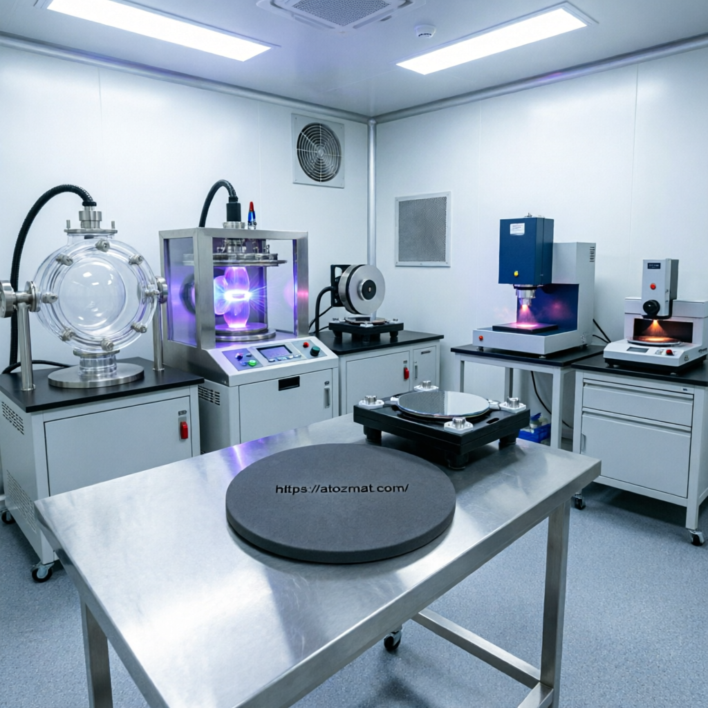
Research laboratory application context for Copper Selenide Sputtering Targets (CuSe2 Sputtering Targets) | CuSe2-ST
Deposition Parameters and Film Quality
Sputtering copper selenide requires careful attention to process parameters. Typical RF or DC magnetron sputtering conditions for CuSe2 targets include substrate temperatures ranging from room temperature to 400°C, with many researchers finding optimal film quality between 200-350°C. Deposition rates generally fall in the 5-30 nm/min range depending on power density and target-to-substrate distance.
Chamber pressure significantly affects film microstructure. Lower pressures (0.3-1 Pa) tend to produce denser films with better adhesion, while slightly higher pressures (2-5 Pa) can improve stoichiometry control by reducing preferential resputtering of selenium. Argon is the standard sputtering gas, though some research groups introduce small amounts of hydrogen or selenium vapor to compensate for selenium loss during deposition.
Film thickness uniformity becomes particularly important for device applications. Most research-scale depositions target films between 100-1000 nm thick, with uniformity better than ±5% across 25-50 mm substrates. Thicker films may develop stress-related defects, while very thin films often show incomplete coverage and island growth morphology.
Emerging Applications in Energy Conversion
The photovoltaic research community has shown growing interest in copper selenide as both an absorber layer and a back contact material. In thin film solar cells, CuSe2 films can serve as hole transport layers or buffer layers, with researchers reporting promising interface properties when paired with cadmium telluride or copper indium gallium selenide absorbers. The material’s work function and carrier concentration can be tuned through deposition conditions and post-treatment, making it adaptable to different device architectures.
Thermoelectric applications represent another active research area. Copper selenide compounds exhibit relatively high Seebeck coefficients and low thermal conductivity, characteristics favorable for waste heat recovery. Recent studies have explored nanostructuring approaches and doping strategies to enhance the thermoelectric figure of merit, with sputtered films offering advantages in terms of composition control and scalability compared to bulk synthesis methods.
Optical and Electronic Properties
As-deposited CuSe2 films typically show optical bandgaps in the 1.2-1.8 eV range, though this varies with stoichiometry and crystallinity. The material exhibits strong optical absorption in the visible and near-infrared spectrum, making it suitable for photodetector and photocatalysis research. Electrical resistivity spans several orders of magnitude depending on deposition conditions, from highly conductive (10^-3 Ω·cm) to semiconducting (10^1 Ω·cm) behavior.
Hall effect measurements on sputtered copper selenide films generally confirm p-type conductivity with hole concentrations ranging from 10^17 to 10^20 cm^-3. Mobility values tend to be modest (1-20 cm²/V·s) compared to conventional semiconductors, reflecting the polycrystalline nature of sputtered films and the presence of grain boundary scattering. Researchers working to improve mobility have explored substrate selection, deposition temperature optimization, and post-deposition crystallization treatments.
Target Selection and Quality Considerations
Selecting copper selenide sputtering targets involves several factors beyond basic composition. Target density affects sputtering yield and film uniformity—higher density targets (typically >95% theoretical density) generally provide more stable deposition rates and better particle performance. Grain size and microstructure influence target behavior during extended sputtering runs, with finer-grained targets often showing more uniform erosion patterns.
Purity requirements depend on the application. For fundamental research and device prototyping, targets with 99.9% (3N) purity often suffice. More demanding applications, particularly those involving electronic devices or optical coatings where trace impurities could affect performance, may require 99.99% (4N) or higher purity levels. Common impurities to monitor include oxygen, carbon, and metallic contaminants from target fabrication.
Target bonding and backing plate selection matter for thermal management and process stability. Copper selenide’s relatively low thermal conductivity means heat dissipation during sputtering can be challenging. Indium or elastomer bonding to copper or molybdenum backing plates helps maintain target temperature control, reducing the risk of thermal stress cracking during high-power operation.
Common Deposition Challenges
Selenium loss during sputtering represents a persistent challenge. The higher vapor pressure of selenium compared to copper means films can become copper-rich unless deposition conditions are carefully controlled. Some research groups address this by using slightly selenium-rich targets or by introducing selenium vapor into the chamber during deposition. Post-deposition selenization in selenium or hydrogen selenide atmospheres can also restore stoichiometry, though this adds process complexity.
Film adhesion to certain substrates can be problematic, particularly on glass or oxide surfaces. Thin adhesion layers of chromium, titanium, or molybdenum (5-20 nm) are commonly used to improve film adhesion and provide better nucleation sites. The choice of adhesion layer can influence film stress and crystallographic orientation, so compatibility testing is advisable for new substrate-film combinations.
Oxidation sensitivity requires attention during both deposition and post-processing. Copper selenide films can oxidize when exposed to air at elevated temperatures, forming copper oxide and selenium oxide phases that degrade electronic properties. Researchers typically use inert atmosphere handling or protective capping layers when thermal treatments are necessary.
Current Research Directions
The materials science community continues to explore composition tuning and doping strategies for copper selenide films. Substitutional doping with elements like aluminum, indium, or sulfur has shown promise for modifying carrier concentration and bandgap. Multi-layer structures combining copper selenide with other chalcogenides are being investigated for tandem solar cells and advanced photodetector designs.
Interface engineering represents another active area. Understanding and controlling the interfaces between copper selenide and adjacent layers—whether transparent conductors, absorber materials, or metal contacts—remains critical for device performance. Sputtering’s ability to produce clean, well-defined interfaces makes it a valuable tool for this research.
Scalability studies are beginning to emerge as copper selenide transitions from purely academic interest toward potential commercial applications. Questions around target lifetime, deposition rate uniformity over large areas, and process reproducibility are receiving increased attention from groups working on pilot-scale demonstrations.
Practical Sourcing Considerations
Copper selenide sputtering targets are available in standard research sizes, commonly including 1-inch, 2-inch, 3-inch, and 4-inch diameter formats with thicknesses of 1/8 inch or 1/4 inch. Custom sizes and bonding configurations can typically be fabricated to match specific deposition system requirements, though lead times may be longer for non-standard geometries.
When evaluating suppliers, inquire about target fabrication methods, as hot pressing, sintering, and melting approaches can produce different microstructures. Certificates of analysis documenting composition and purity provide important quality assurance. Some suppliers offer target characterization services including density measurement, grain size analysis, and impurity profiling.
Storage and handling practices affect target performance. Copper selenide should be stored in dry, inert conditions to minimize surface oxidation. Targets should be inspected for cracks, chips, or bonding defects before installation, as these can lead to arcing or particle generation during sputtering.
Conclusion
Copper selenide sputtering targets enable researchers and engineers to explore a versatile thin film material system with applications spanning photovoltaics, thermoelectrics, and optoelectronics. Success with CuSe2 deposition requires attention to stoichiometry control, thermal management, and interface quality. As research continues to advance understanding of copper selenide’s properties and processing requirements, the material’s role in next-generation energy and electronic devices is likely to expand.
For laboratories and research groups working with copper selenide thin films, selecting high-quality targets from reliable suppliers forms the foundation for reproducible results and meaningful materials development.
Product Information
For more information about copper selenide sputtering targets, including available sizes and specifications, visit:
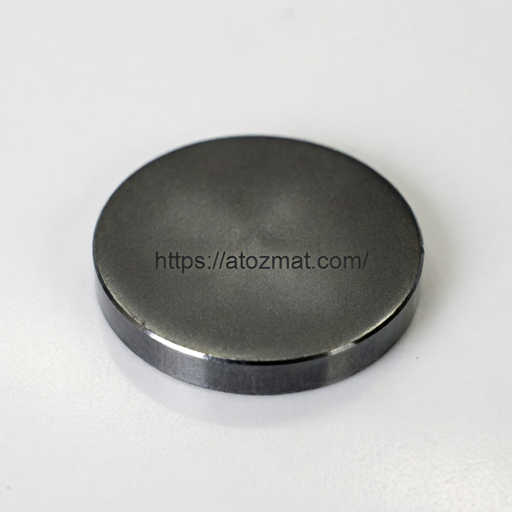
Aluminum boride (AlB6) sputtering targets have gained attention in materials research and advanced coating applications due to the compound’s unique combination of hardness, thermal stability, and electrical properties. Engineers working on protective coatings, wear-resistant surfaces, and experimental semiconductor materials increasingly consider AlB6 thin films for applications where conventional materials face performance limitations. Understanding the deposition parameters, film characteristics, and application-specific requirements helps researchers and process engineers achieve consistent, high-quality results.
Aluminum boride exists in several stoichiometric forms, with AlB6 representing a boron-rich composition that exhibits exceptional hardness and chemical stability. The material’s crystal structure contributes to mechanical properties that make deposited films attractive for protective coating applications. Unlike pure aluminum or simple aluminum alloys, AlB6 targets produce films with significantly enhanced wear resistance and thermal stability.
The boron-rich composition presents specific challenges during target fabrication and sputtering. Material brittleness requires careful handling during manufacturing and installation. Target purity typically ranges from 99.5% to 99.9%, with oxygen and carbon representing the most common impurities. These trace contaminants can affect film stoichiometry and properties, making target quality a critical selection factor for research applications.
Research laboratory application context for Aluminum Boride Sputtering Targets (AlB6 Sputtering Targets) | AlB6-ST
Deposition Parameters and Film Quality
Researchers working with AlB6 targets typically operate within specific parameter windows to achieve desired film properties. Substrate temperatures commonly range from room temperature to 500°C, with higher temperatures generally promoting better crystallinity and film adhesion. However, temperature selection depends heavily on substrate compatibility and intended application.
Sputtering power density affects both deposition rate and film composition. Research groups typically report deposition rates between 5 and 30 nm/min for DC magnetron sputtering, depending on power settings, target-to-substrate distance, and working pressure. RF sputtering may be preferred for insulating substrates, though deposition rates tend to be lower.
Working pressure and gas composition significantly influence film properties. Most AlB6 deposition occurs in pure argon atmospheres at pressures between 2 and 10 mTorr. Reactive sputtering with nitrogen or oxygen additions has been explored for property modification, though this can complicate stoichiometry control. Base pressure before deposition typically needs to reach at least 1×10⁻⁶ Torr to minimize contamination from residual gases.
Film Properties and Characterization
AlB6 thin films deposited under optimized conditions exhibit hardness values ranging from 20 to 35 GPa, depending on deposition parameters and post-deposition treatment. This positions aluminum boride films between conventional hard coatings like TiN (20-25 GPa) and ultra-hard materials like cubic boron nitride. The exact hardness achieved depends on film density, grain structure, and residual stress.
Electrical resistivity of AlB6 films varies considerably with deposition conditions. Values reported in research literature range from 10⁻⁴ to 10⁻² Ω·cm, making the material suitable for applications requiring moderate conductivity. This electrical behavior distinguishes AlB6 from insulating borides and enables potential use in electronic device structures.
Thermal stability represents another key advantage. AlB6 films maintain structural integrity at temperatures exceeding 800°C in inert atmospheres, though oxidation becomes a concern above 500°C in air. This thermal stability makes the material attractive for high-temperature protective coatings and applications involving thermal cycling.
Primary Application Areas
Hard protective coatings represent the most established application for AlB6 thin films. The combination of high hardness, chemical stability, and moderate electrical conductivity makes these films suitable for cutting tools, wear-resistant surfaces, and protective layers on mechanical components. Research continues on optimizing film adhesion and residual stress for industrial coating applications.
Semiconductor research groups investigate AlB6 films for specialized electronic applications. The material’s electrical properties and thermal stability make it a candidate for diffusion barriers, contact materials, and experimental device structures. While not yet widely adopted in commercial semiconductor manufacturing, ongoing research explores potential advantages over conventional barrier materials.
Optical coating applications leverage AlB6’s reflective properties in specific wavelength ranges. The material shows promise for infrared reflective coatings and specialized optical filter applications, though this remains an emerging area compared to established coating materials.
Energy-related research includes investigation of AlB6 films for thermoelectric applications and as components in advanced battery systems. The material’s electrical and thermal properties suggest potential advantages, though practical implementation requires further development.
Selection and Procurement Considerations
Engineers selecting AlB6 sputtering targets should prioritize purity specifications appropriate for their application. Research-grade work typically requires 99.9% purity or higher, while some protective coating applications may accept 99.5% material. Detailed impurity analysis is important, particularly for oxygen, carbon, and metallic contaminants.
Target dimensions must match the deposition system configuration. Common research-scale sizes include 2-inch and 3-inch diameter targets with thicknesses of 1/8 inch or 1/4 inch. Larger production systems may require 4-inch or custom-sized targets. Backing plate bonding becomes increasingly important for larger targets to ensure thermal management and mechanical stability during sputtering.
Target density affects sputtering behavior and film quality. Higher-density targets generally provide more consistent sputtering rates and better film uniformity. Relative density (typically 95-99% of theoretical density) and grain structure characteristics are important specifications to review.
Lead times for AlB6 targets can be substantial due to specialized fabrication requirements. Engineers should plan procurement well in advance of experimental schedules. Establishing relationships with suppliers experienced in boride materials helps ensure consistent quality and technical support.
Common Deposition Challenges
Target cracking represents a frequent issue with brittle boride materials. Thermal stress during sputtering can propagate cracks, particularly in targets with pre-existing flaws or inadequate bonding. Gradual power ramping and proper cooling help minimize thermal shock. Some research groups pre-condition new targets with extended low-power sputtering before full-power operation.
Film adhesion to substrates requires careful attention to surface preparation and deposition conditions. Substrate cleaning, plasma etching, and thin interlayer deposition can improve adhesion for challenging substrate materials. Residual stress in thick films may cause delamination if not properly managed through deposition parameter optimization.
Stoichiometry control presents challenges due to preferential sputtering of aluminum versus boron. Film composition may deviate from target composition, particularly at higher power densities. Researchers often need to characterize deposited films using techniques like X-ray photoelectron spectroscopy or Rutherford backscattering to verify composition.
Contamination from residual gases or target surface oxidation can degrade film properties. Maintaining low base pressure, using high-purity process gases, and implementing target pre-sputtering routines help minimize contamination. Some groups use in-situ target cleaning procedures between deposition runs.
Current Research Directions
Materials scientists continue investigating composition modifications and doping strategies to tailor AlB6 film properties. Co-sputtering with other materials or reactive sputtering with nitrogen has shown potential for property enhancement. Understanding structure-property relationships in these modified films remains an active research area.
Interface engineering between AlB6 films and various substrate materials receives ongoing attention. Optimizing adhesion layers, understanding interfacial reactions, and controlling stress at interfaces are critical for practical applications. Research groups explore different interlayer materials and deposition sequences to improve overall coating performance.
Scale-up from laboratory deposition to larger-area coating processes presents technical challenges. Maintaining film uniformity, managing target utilization, and ensuring process reproducibility become more complex at production scales. Development work continues on optimizing deposition system configurations and process parameters for larger substrates.
Making the Right Choice
AlB6 sputtering targets offer unique property combinations for researchers and engineers working on advanced coating applications. The material’s hardness, thermal stability, and electrical characteristics enable applications where conventional materials fall short. Success requires careful attention to target quality, deposition parameter optimization, and application-specific requirements.
Engineers should evaluate whether AlB6’s specific properties justify the material’s higher cost and processing complexity compared to more established coating materials. For applications requiring exceptional hardness combined with moderate conductivity and high-temperature stability, aluminum boride films provide compelling advantages. Research applications benefit from the material’s unique property space for fundamental studies and device development.
Working with experienced materials suppliers and leveraging published research helps accelerate process development and troubleshooting. As understanding of AlB6 thin film deposition continues to advance, the material’s application range will likely expand beyond current protective coating and research uses.
Product Availability
Engineers and researchers interested in aluminum boride sputtering targets can find detailed specifications and ordering information through specialized materials suppliers. AlB6 sputtering targets are available from atozmat in various sizes and configurations for research and production applications.
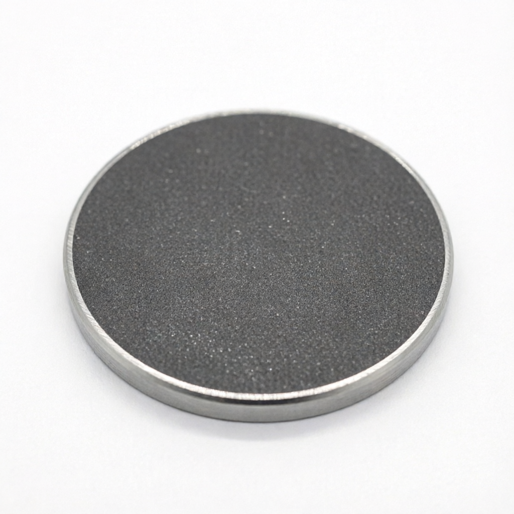
Aluminum doped zinc oxide (AZO) has become a widely used transparent conductive oxide material in thin film deposition processes. Engineers and materials specialists working on optoelectronic devices, solar cells, flat panel displays, and functional coatings often turn to AZO sputtering targets when they need a cost-effective alternative to indium tin oxide (ITO) with comparable electrical and optical performance.
Aluminum doped zinc oxide is a ceramic compound where small amounts of aluminum oxide (Al₂O₃) are incorporated into a zinc oxide (ZnO) matrix. The aluminum acts as an n-type dopant, increasing the material’s electrical conductivity while maintaining high optical transparency in the visible spectrum. This combination makes AZO particularly valuable for applications requiring both electrical function and light transmission.
In sputtering processes, AZO targets are typically manufactured from 99.99% purity material. The doping level and microstructure affect film properties, so target density and grain uniformity matter for consistent deposition results. Most industrial AZO targets are produced through ceramic powder processing methods that control composition and minimize contamination.
The primary advantage of AZO over ITO is cost. Indium is a relatively scarce and expensive element, while zinc and aluminum are abundant and economical. For large-area coating applications or high-volume production environments, this cost difference becomes significant. AZO also offers better thermal stability than ITO in some processing conditions, making it suitable for applications involving elevated substrate temperatures.
Common applications include:
Transparent electrodes for thin film solar cells and photovoltaic research
Conductive layers in flat panel displays and touch screen assemblies
Antireflective and conductive coatings for optoelectronic devices
Functional films in sensor development and materials research
Low-emissivity architectural glass coatings
Engineers working with AZO typically use magnetron sputtering or RF sputtering techniques. Film properties such as resistivity, carrier concentration, and optical transmittance depend on deposition parameters including power density, substrate temperature, working pressure, and oxygen partial pressure during the process.
Technical Considerations for AZO Sputtering
AZO is a brittle ceramic material, which affects both target handling and process behavior. Thermal shock during high-power sputtering can cause target cracking if power ramp rates are too aggressive. Many users bond AZO targets to copper backing plates to improve thermal management and mechanical stability during deposition.
Oxygen content in the sputtering atmosphere significantly influences film stoichiometry and electrical properties. Too much oxygen can reduce conductivity, while insufficient oxygen may lead to metallic zinc formation and poor film quality. Process engineers typically optimize the oxygen-to-argon ratio based on their specific equipment and application requirements.
Film adhesion to various substrate materials is another practical concern. Surface preparation, substrate cleaning, and the use of adhesion-promoting interlayers can all affect coating performance and durability in the final application.
Common Target Sizes and Sourcing Considerations
AZO sputtering targets are available in circular, rectangular, and custom geometries. Common circular sizes include:
1 inch diameter × 1/8 inch thick
1 inch diameter × 1/4 inch thick
2 inch diameter × 1/8 inch thick
2 inch diameter × 1/4 inch thick
3 inch diameter × 1/8 inch thick
3 inch diameter × 1/4 inch thick
4 inch diameter × 1/8 inch thick
4 inch diameter × 1/4 inch thick
Metric equivalents such as 50 mm, 60 mm, 80 mm, and 100 mm diameters are also standard in many markets. Thickness choices depend on the deposition system design and the total material utilization required before target replacement.
When sourcing AZO targets, buyers typically evaluate material purity, target density, dimensional tolerance, backing plate bonding quality, and consistency across batches. Lead times can vary depending on whether standard or custom sizes are needed. For research applications, smaller targets are often sufficient, while production environments may require larger formats or multiple targets for continuous operation.
Selection Factors and Trade-Offs
Choosing between AZO and other transparent conductive oxides involves several trade-offs. ITO generally offers lower resistivity and higher optical transparency, but at significantly higher material cost. Fluorine-doped tin oxide (FTO) provides excellent chemical and thermal stability but typically has higher resistivity than AZO.
For cost-sensitive applications where moderate conductivity is acceptable, AZO often represents the best balance. For applications requiring the lowest possible sheet resistance or the highest optical clarity, ITO may still be preferred despite the cost premium.
Doping level is another selection factor. Higher aluminum content generally increases conductivity but can reduce optical transparency and may affect film stress and adhesion. Standard doping levels are typically available, though custom compositions can be sourced for specialized research or production needs.
Current Research Directions
Ongoing thin film research continues to explore composition tuning, interface engineering, and process optimization for AZO films. Areas of active investigation include improving film conductivity through microstructure control, enhancing stability under environmental exposure, and developing deposition processes compatible with flexible substrates and low-temperature processing.
In semiconductor and energy research, AZO is being evaluated for emerging applications in next-generation photovoltaics, transparent electronics, and functional sensor systems. These research directions aim to expand the performance envelope of AZO while maintaining its cost and availability advantages.
Practical Recommendations
For engineers new to AZO sputtering, starting with standard target sizes and well-documented deposition parameters helps establish a baseline process. Once stable deposition is achieved, systematic optimization of power, pressure, temperature, and gas composition can improve film properties for specific applications.
Maintaining consistent target surface condition and avoiding contamination during handling are important for reproducible results. Regular target cleaning and proper storage between deposition runs help minimize particle generation and film defects.
For production environments, establishing a reliable supply chain with consistent target quality is essential. Batch-to-batch variation in target density or composition can affect process stability and film uniformity, so qualification procedures and incoming material inspection are worthwhile investments.
Conclusion
Aluminum doped zinc oxide sputtering targets provide a practical, cost-effective solution for transparent conductive film deposition across a wide range of applications. Understanding the material’s properties, process sensitivities, and application trade-offs helps engineers and buyers make informed decisions about when AZO is the right choice for their thin film needs.
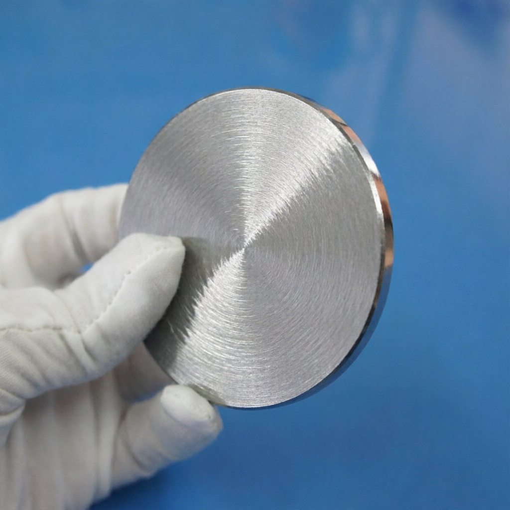
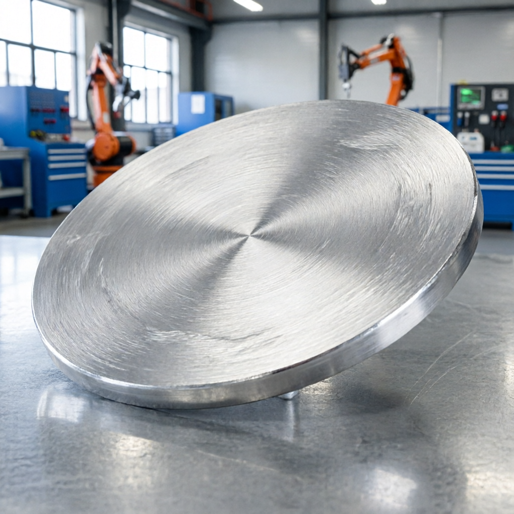
Aluminum sputtering targets are high-purity aluminum source materials used in physical vapor deposition (PVD) processes to deposit thin aluminum films onto substrates. These targets serve as the material source in sputtering systems, where energetic ions bombard the target surface and eject aluminum atoms that then condense onto the substrate as a thin film. The quality, purity, and physical characteristics of the target directly influence film uniformity, contamination levels, and overall process stability.
In industrial thin film deposition, aluminum targets are valued for their combination of electrical conductivity, reflectivity, and relatively straightforward processing behavior. Engineers and materials specialists use aluminum films across semiconductor interconnects, optical reflectors, protective coatings, and research-scale materials development. Understanding target specifications, common sizing conventions, and selection factors helps buyers make informed sourcing decisions.
Aluminum offers several practical advantages in thin film applications. Its high electrical conductivity makes it a common choice for metallization layers in microelectronics and semiconductor devices. The material’s natural oxide layer can provide corrosion resistance in certain coating applications, while its high reflectivity supports optical and decorative coating work. Aluminum films are also relatively easy to pattern and etch compared to some refractory metals, which simplifies device fabrication processes.
From a deposition perspective, aluminum sputters at moderate power levels and generally produces uniform films when target quality and system parameters are properly controlled. The material’s relatively low melting point compared to metals like tungsten or molybdenum means that thermal management during sputtering is less demanding, though it also requires attention to avoid localized overheating or target cracking during high-power operation.
Aluminum sputtering targets are commonly produced at 99.999% purity (5N grade). This purity level helps minimize contamination in deposited films, which is critical in semiconductor and precision optical applications where trace impurities can degrade electrical performance or optical clarity. Higher purity grades may be specified for advanced research or ultra-sensitive device applications, though 5N material meets the requirements of most industrial thin film processes.
Beyond chemical purity, target microstructure and density affect sputtering behavior. Targets with uniform grain structure and high relative density tend to sputter more consistently and produce fewer particulates during deposition. Manufacturing methods such as powder metallurgy, casting, or rolling can influence these characteristics, and buyers working on critical applications often request material certifications or process documentation to verify target quality.
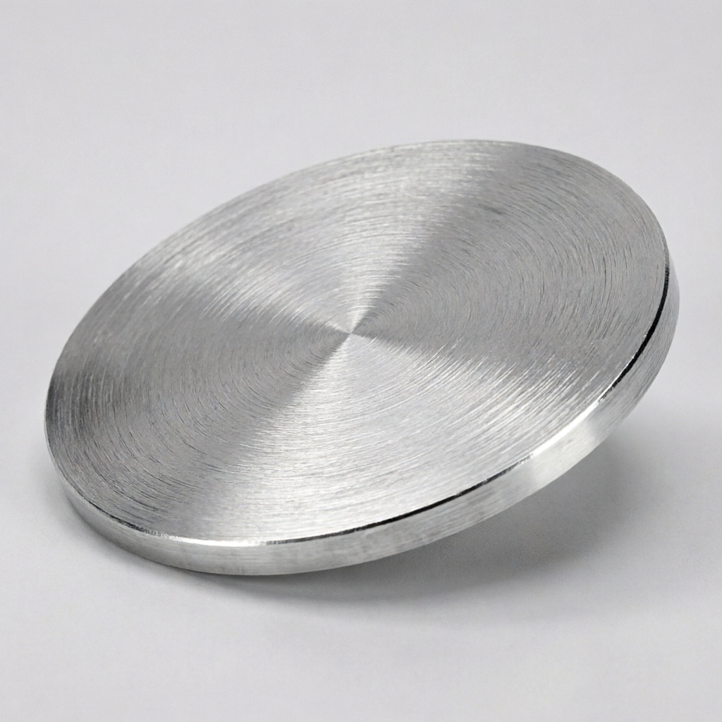
Common Target Sizes and Configurations
Aluminum sputtering targets are available in various shapes including circular disks, rectangular plates, and custom geometries to match specific deposition system requirements. Circular targets are widely used in research and small-scale production environments. Common circular sizes include:
1 inch diameter × 1/8 inch thick
1 inch diameter × 1/4 inch thick
2 inch diameter × 1/8 inch thick
2 inch diameter × 1/4 inch thick
3 inch diameter × 1/8 inch thick
3 inch diameter × 1/4 inch thick
4 inch diameter × 1/8 inch thick
4 inch diameter × 1/4 inch thick
Metric equivalents such as 50 mm, 60 mm, 80 mm, and 100 mm diameters are also common in international markets. Thickness choices typically range from 3 mm to 6 mm, with thicker targets offering longer operational life before replacement becomes necessary. Larger rectangular or custom-shaped targets are used in production-scale coating systems where substrate size or throughput requirements demand larger source material areas.
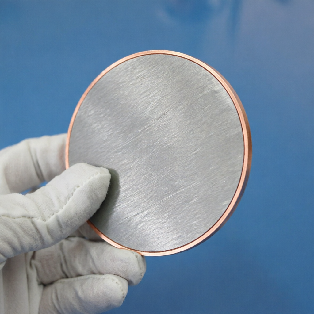
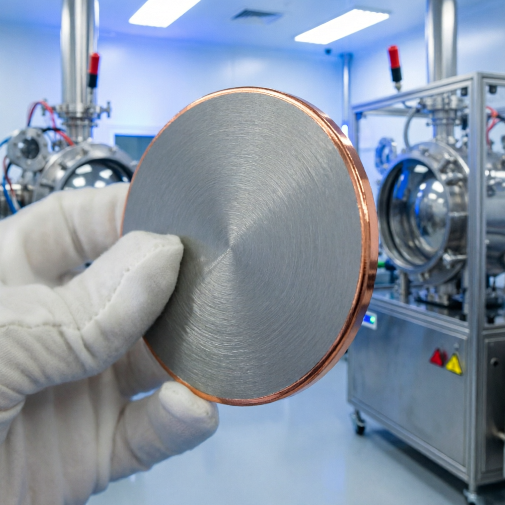
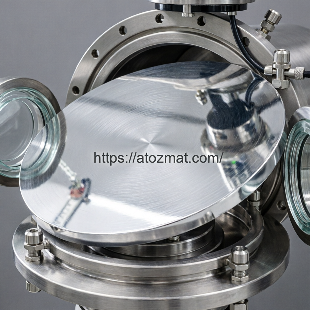
Backing Plates and Bonding Options
Many sputtering systems require targets to be bonded to a backing plate, typically made of copper or another thermally conductive material. The backing plate provides mechanical support, improves thermal management during sputtering, and allows secure mounting in the deposition chamber. Bonding methods include diffusion bonding, elastomer bonding, and soldering, each with trade-offs in thermal conductivity, ease of target replacement, and cost.
Engineers selecting bonded targets should consider the thermal expansion match between aluminum and the backing material, as mismatches can lead to stress, warping, or debonding during thermal cycling. Copper backing is common due to its high thermal conductivity and reasonable cost, though some systems use alternative materials depending on process requirements.
Applications Across Industries
Aluminum thin films appear in a wide range of industrial and research applications. In semiconductor manufacturing, aluminum serves as an interconnect material in integrated circuits, though it has been partially replaced by copper in advanced nodes. The material remains relevant in legacy processes, power devices, and certain analog applications where its processing simplicity and cost-effectiveness are advantageous.
Optical coatings represent another major application area. Aluminum’s high reflectivity in the visible and near-infrared spectrum makes it suitable for mirrors, reflectors, and decorative coatings. The material is also used in packaging films, where thin aluminum layers provide moisture and gas barriers for food and pharmaceutical products.
In research environments, aluminum sputtering targets support materials science studies, sensor development, and thin film property investigations. The material’s well-characterized behavior and availability make it a practical choice for laboratory-scale deposition work and process development.
Selection Factors for Engineers and Buyers
When sourcing aluminum sputtering targets, engineers typically evaluate several factors:
Purity requirements: Match target purity to application sensitivity and contamination tolerance.
Size and geometry: Ensure target dimensions fit the deposition system and provide adequate material for the intended number of deposition runs.
Backing and bonding: Determine whether a bonded target is required and select appropriate backing material and bonding method.
Surface finish: Specify surface roughness or finish requirements if film quality or particulate control is critical.
Lead time and supply consistency: Evaluate supplier reliability, especially for ongoing production needs.
Cost considerations also play a role, particularly in high-volume production environments. While aluminum is generally less expensive than many other sputtering target materials, total cost of ownership includes target life, deposition rate, and process yield, not just initial purchase price.
Common Technical Challenges
Aluminum’s relatively low melting point can lead to localized melting or target damage if sputtering power is too high or cooling is inadequate. This is especially relevant in DC magnetron sputtering, where power density at the target surface can be significant. Proper system setup, power ramping, and cooling management help avoid these issues.
Oxidation is another consideration. Aluminum readily forms a thin oxide layer when exposed to air, which can affect initial sputtering behavior and film properties. Pre-sputtering or target conditioning steps are often used to remove surface oxides before depositing films onto substrates. In reactive sputtering processes where aluminum oxide films are desired, controlled oxygen introduction allows formation of Al₂O₃ coatings with tailored stoichiometry and properties.
Target utilization and erosion patterns also matter for process consistency. Non-uniform erosion can lead to changes in deposition rate and film uniformity over the target’s operational life. Magnetron design, target rotation, and periodic target replacement help maintain stable process conditions.
Current Directions in Aluminum Thin Film Work
Ongoing thin film research continues to explore aluminum-based material systems for emerging applications. Interface engineering between aluminum and other materials is an active area, particularly in multilayer optical coatings and electronic device structures. Researchers are also investigating aluminum alloy targets and co-sputtering approaches to tune film properties for specific functional requirements.
In industrial settings, process optimization efforts focus on improving deposition uniformity, reducing particulate contamination, and extending target life. These practical improvements support cost reduction and quality enhancement in production environments.
Practical Sourcing Considerations
Buyers sourcing aluminum sputtering targets should request material certifications that document purity, composition, and manufacturing process details. For critical applications, sample testing or qualification runs help verify that a particular target lot meets performance requirements before committing to larger purchases.
Custom target sizes and geometries are often available to match specific system configurations or application needs. Lead times for custom targets can be longer than for standard sizes, so planning ahead is important for projects with tight schedules.
Establishing relationships with reliable suppliers helps ensure consistent material quality and responsive technical support. Suppliers with experience in thin film applications can often provide guidance on target selection, bonding options, and process troubleshooting.
Conclusion
Aluminum sputtering targets are versatile source materials that support a wide range of thin film deposition applications. Their combination of electrical conductivity, optical properties, and processing simplicity makes them valuable in semiconductor, optical, and coating industries. Understanding purity requirements, common sizing conventions, backing options, and selection factors helps engineers and buyers make informed decisions that balance performance, cost, and supply reliability.
For applications requiring high-purity aluminum targets with consistent quality, working with experienced suppliers and specifying clear material requirements ensures successful thin film deposition outcomes.
Product Information
High-purity aluminum sputtering targets in standard and custom sizes are available from atozmat. For detailed specifications, pricing, and ordering information, visit: